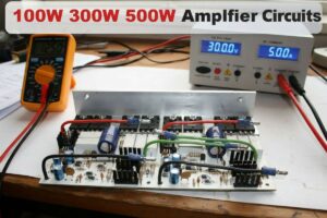
The TDA7385 amplifier circuit is a 4-channel car amplifier application that operates with a single supply. Thanks to its 12-18 V DC supply, 4 Ω speaker outputs, standby and mute control, it is suitable for in-car audio systems, portable speakers, and small audio projects powered by 12 V.
Basic Structure of the Circuit
Contents
- 1 Basic Structure of the Circuit
- 2 Circuit Blocks
- 3 Power Supply Stage and Current Requirement
- 4 Connection of the Audio Inputs
- 5 Standby and Mute Controls
- 6 SVR, AC-GND, and Grounding Points
- 7 Why Are the TDA7385 Speaker Outputs Not Connected to the Chassis?
- 8 About Output Power
- 9 Technical Specifications
- 10 Component List
- 11 Points to Consider During Assembly
- 12 First Startup and Test
- 13 Common Faults and Their Symptoms
- 14 Safety and Usage Notes
- 15 In Which Applications Can It Be Preferred?
TDA7385 4-channel car amplifier circuit diagram
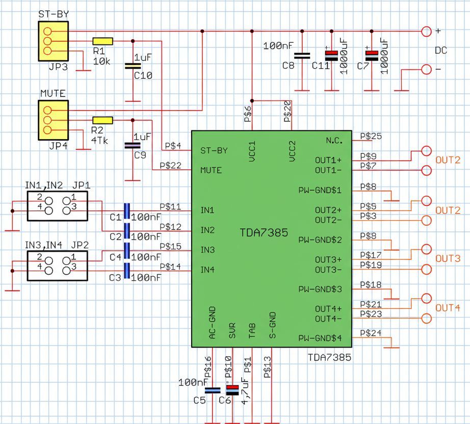
At the center of the circuit is the TDA7385 integrated circuit, shown as US1. This IC combines four bridge-output power amplifiers in the same package.
Each channel has a separate input capacitor and a separate speaker output pair. Since the outputs are bridge-connected, both terminals of the speaker are driven by the IC.
The TDA7385 operates in class AB structure. Unlike class D amplifiers, it does not require a high-frequency switching filter at the output; however, its efficiency is lower and the IC can heat up significantly. Therefore, a suitable heatsink is not optional in this circuit; it is a basic requirement.
Circuit Blocks
| Block | Components | Function |
|---|---|---|
| Supply and filtering | C7, C8, C11 | Suppresses sudden current demands and noise on the 12-18 V DC supply line. |
| Audio inputs | JP1, JP2, C1, C2, C3, C4 | Transfers the four audio channels to the TDA7385 inputs by blocking the DC component. |
| Standby control | JP3, R1, C10 | Wakes the IC from sleep mode or puts it into low-consumption standby mode. |
| Mute control | JP4, R2, C9 | Mutes the audio output with a simple jumper, without software. |
| Reference and noise suppression | C5, C6 | Filters the AC-GND and SVR pins, reducing the risk of hum and turn-on noise. |
| Speaker outputs | OUT1, OUT2, OUT3, OUT4 | Provides a separate bridge-output speaker connection for each channel. |
Power Supply Stage and Current Requirement
The circuit operates with a single DC supply in the 12-18 V range from the +DC and -DC terminals. It is suitable for use with a car battery; however, if it will be connected directly to the battery, a fuse must definitely be added to the supply line. The fuse should be positioned as close to the battery as possible.
C7 and C11 1000 µF electrolytic capacitors reduce low-frequency supply ripple.
The C8 100 nF capacitor acts as a local bypass against fast current pulses and high-frequency noise.
In power amplifiers, these two capacitor types do not replace each other; while the large electrolytic behaves like an energy reservoir, the 100 nF capacitor transfers fast noise to ground through a short path.
If the supply cables are chosen too thin, the voltage drops during bass hits, the sound becomes distorted, and the IC heats up unnecessarily.
If all 4 channels will operate at the same time, the cable cross-section, fuse rating, and power supply current should be considered together.
If a laboratory adapter is used, the output power will remain lower than expected with weak adapters that enter current limiting.
Connection of the Audio Inputs
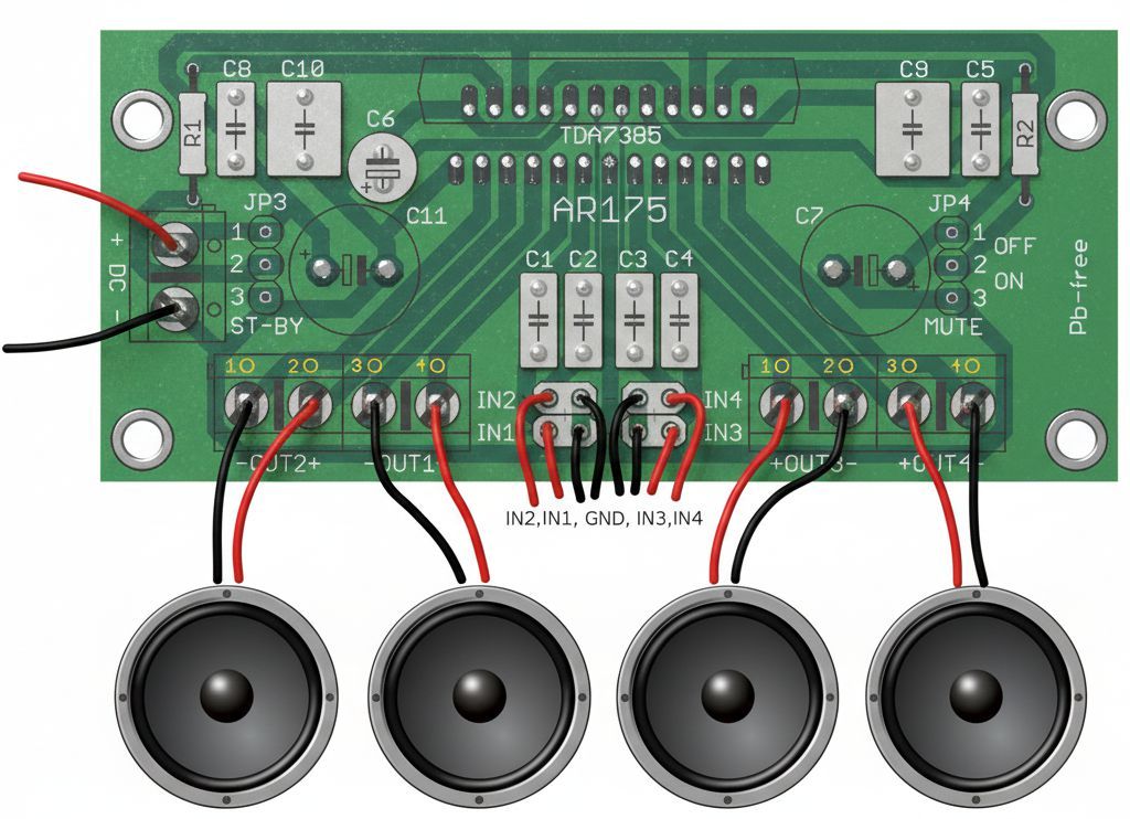
JP1 and JP2 connectors are used for the four channel inputs. In the schematic, the IN1, IN2, IN3, and IN4 inputs go to the TDA7385 input pins through C1-C4.
These capacitors have a value of 100 nF and block the DC component at the input. Thus, small DC offsets that may come from the source device are not transferred directly to the power stage.
Using shielded cable on the input line makes a difference in practice. Especially inside a vehicle, the ignition system, alternator, fan motor, and long cable routes can be sources of noise.
The signal ground should be connected to the power ground at the same point, and the input cables should not be routed for long distances parallel to the speaker and supply cables.
For simpler single-channel applications, the TDA2003 mono amplifier circuit can be tried with fewer components and lower power.
The TDA7385 provides a more organized solution when four channels need to be combined in a single IC.
Standby and Mute Controls
Standby Input
JP3 controls the ST-BY input of the TDA7385. When the jumper is in the 1-2 position, standby is disabled and the amplifier becomes ready to operate.
If the jumper is moved to the 2-3 position, the ST-BY line is pulled to the passive state and the IC enters sleep mode.
R1 10 kΩ and C10 1 µF create a short delay on the standby line. This delay prevents the IC from turning on suddenly the moment the supply is applied.
Softening the startup sequence in power amplifiers helps reduce the disturbing “pop” sound coming from the speaker.
Mute Input
JP4 controls the MUTE line. When the jumper is in the 1-2 position, the sound is on; in the 2-3 position, the outputs are muted.
R2 47 kΩ and C9 1 µF prevent the mute line from changing level quickly and uncontrollably.
The mute input is used only to cut the sound; it does not turn the IC off completely. In systems that will not be used for a long time, standby should be preferred.
Mute is more suitable for source selection, startup waiting, or temporarily muting the speaker during testing.
SVR, AC-GND, and Grounding Points
The C6 4,7 µF capacitor is connected to the SVR pin. This pin is related to the reference voltage structure inside the IC, and if it is not filtered well, hum, background noise, or a turn-on sound pulse may occur.
It should be remembered that C6 is polarized, and its positive and negative orientation should be installed according to the marking on the PCB.
The C5 100 nF capacitor filters the AC-GND line. The schematic also shows that the TAB and S-GND terminals are connected to ground.
In multi-channel power ICs such as the TDA7385, routing the signal ground and power ground randomly causes noise.
In PCB design, high-current speaker returns and low-level input ground should be kept as separate as possible.
Why Are the TDA7385 Speaker Outputs Not Connected to the Chassis?
Each of the OUT1, OUT2, OUT3, and OUT4 outputs consists of two terminals: OUT+ and OUT-. These outputs are bridge-type.
One terminal of the speaker is connected to the OUT+ line, and the other terminal is connected to the OUT- line. The negative terminal of the speaker must never be connected to the vehicle chassis or the circuit GND line.
This mistake is frequently seen in some old speaker wiring removed from car stereos.
Installations using a common chassis are not suitable for bridge-output ICs such as the TDA7385.
An incorrect connection short-circuits the output transistors, overheats the IC, and may cause permanent damage.
The speaker impedance should be considered as 4 Ω. Lower-impedance speakers, especially at high volume, may cause the IC to enter overcurrent or thermal protection.
Loading a single channel by connecting two speakers in parallel is not a correct method.
About Output Power
The circuit is introduced with a maximum output power of 4×42 W; this value is valid for a 4 Ω load and suitable supply conditions.
In class AB bridge amplifiers powered by a car battery, continuous RMS power is lower depending on supply voltage, cooling, distortion limit, and speaker impedance.
In practice, this type of IC is suitable for driving door speakers or small enclosures.
For loads such as subwoofers that require high current at low frequencies, a larger heatsink, stronger supply, and suitable enclosure are required.
For high-power bass applications, different topologies such as a TDA7294 car subwoofer amplifier may be a more correct choice.
Technical Specifications
| Feature | Value / Description |
|---|---|
| IC | TDA7385 |
| Amplifier type | 4-channel class AB power amplifier |
| Supply voltage | 12-18 V DC single supply |
| Output power | 4×42 W / 4 Ω maximum |
| Speaker connection | Bridge output, OUT+ and OUT- for each channel |
| Control inputs | Standby and mute |
| Protection | Thermal and short-circuit protection |
| PCB size | 80×35 mm |
Component List
| Reference | Value / Model | Function |
|---|---|---|
| US1 | TDA7385 | 4-channel power amplifier |
| R1 | 10 kΩ | Standby control line |
| R2 | 47 kΩ | Mute control line |
| C1, C2, C3, C4 | 100 nF | Audio input coupling capacitors |
| C5 | 100 nF | AC-GND filtering |
| C6 | 4,7 µF | SVR filtering |
| C7, C11 | 1000 µF | Supply line filtering |
| C8 | 100 nF | Supply bypass capacitor |
| C9 | 1 µF | Mute line delay / filter capacitor |
| C10 | 1 µF | Standby line delay / filter capacitor |
| JP1, JP2 | Input connectors | IN1-IN4 audio inputs |
| JP3 | Standby jumper | Operating / sleep mode selection |
| JP4 | Mute jumper | Sound on / mute selection |
Points to Consider During Assembly
Starting assembly with low-profile components is the cleanest method. First, resistors and small capacitors can be installed, followed by electrolytic capacitors and connectors.
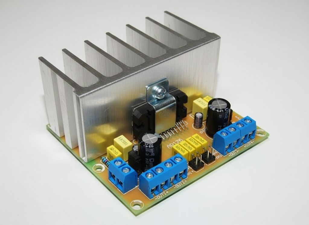
The TDA7385 should be placed on the board after it is fixed to the heatsink. Instead of forcing the IC legs to align, the mechanical fit should be checked first.
The orientation of electrolytic capacitors is important. If C6, C7, C9, C10, and C11 are installed in reverse, the circuit may not work; worse, the capacitor may heat up or be damaged.
Using a current-limited power supply during the first startup allows incorrect soldering or short-circuit faults to be detected before they become larger problems.
Suitable thermal paste should be applied between the heatsink and the IC. The electrical condition of the rear surface of the IC should be checked according to the package and application used, and it should be ensured that the metal heatsink does not touch another point.
First Startup and Test
In the first test, the correct polarity should be checked at the supply terminals before connecting the speakers. Then JP3 is moved to the operating position, and JP4 is moved to the sound-on position. If the IC does not draw excessive current, the speakers can be connected one by one.
A low-level audio signal should be applied to the input and the volume should be increased slowly. If there is no sound on one channel, first the related input capacitor, connector connection, and speaker pair should be checked. If all four channels are silent, the problem is generally on the standby, mute, supply, or common ground connection side.
To compare similar IC examples operating at lower powers, the TDA2005 mono amplifier circuit can be examined. Thus, the difference between a single-channel structure and a multi-channel bridge-output structure can be seen more clearly.
Common Faults and Their Symptoms
| Symptom | Possible Cause | Check Point |
|---|---|---|
| No sound at all | Standby or mute jumper in the wrong position | JP3 and JP4 positions should be checked |
| No sound on a single channel | Input capacitor, connector, or speaker connection faulty | The related IN and OUT line should be traced |
| IC heats up quickly | Speaker output shorted to chassis, low impedance, or insufficient heatsink | OUT+ and OUT- lines should be checked with respect to GND |
| Pop sound at startup | Mute / standby RC line faulty or capacitor orientation incorrect | C9, C10, R1, and R2 should be checked |
| Alternator hum present | Grounding arrangement, input cable, or supply filtering insufficient | Signal ground and power ground connections should be reviewed |
| Distortion at high volume | Supply current insufficient or speaker impedance low | Supply voltage should be measured while the volume is increased |
Safety and Usage Notes
Although a car battery appears to be low-voltage, it can deliver very high current. An incorrect connection can burn the cable, PCB trace, or IC in a short time.
A suitable fuse, sufficient cable cross-section, and solid terminal block should be used on the supply line.
Speaker cables should be insulated so that they do not touch the vehicle body. In a bridge-output amplifier, it is not normal for any of the speaker terminals to touch the chassis.
In larger systems where speaker protection is desired, additional solutions such as a speaker protection circuit can be considered; however, since the output structure in this circuit is bridge-type, the protection circuit to be added must be suitable for this.
In Which Applications Can It Be Preferred?
The TDA7385 circuit is a practical solution in 12 V systems where four 4 Ω speakers need to be driven from a single board.
It can be used in in-car front-rear speaker layouts, small workshop sound systems, portable battery-powered speakers, or desktop amplifier applications powered by a 12 V adapter.
If very high sound pressure, a low-impedance subwoofer, or long-term full-power operation is targeted, this circuit alone may not be sufficient.
In this case, a higher-power amplifier stage, larger heatsink, and stronger power supply are required.
Previously, in the article on 4x car amplifier circuits with the TDA73XX Series, TDA7385-compatible double-sided and single-layer PCBs were shared, but although this design is single-layer, it is quite good in terms of DC filter capacitor placement and similar details.
The PCB drawing was copied from the image using Sprint layout 6. It was checked but not tested. You need to reinforce all traces with solder filling, especially the voltage input and speaker output traces, by soldering wire to make them thicker. The 1000UF filter capacitors should be 16v for 12V supply voltage and 25V for 18V supply voltage.
Source: arlisklep.pl/files/ARLI/AR175.pdf