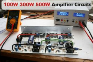
TDA7294 IC: 100W DMOS Amplifier Features. The TDA7294 is a popular Class AB audio power IC with a DMOS output stage, offered by STMicroelectronics in a Multiwatt-15 package and used in Hi-Fi and subwoofer applications. Thanks to its symmetrical supply, mute/stand-by control, and short-circuit/thermal protection structure, it offers a compact solution for 4 Ω and 8 Ω speaker projects, but it requires careful cooling.
TDA7294 Technical Specifications
Contents
- 1 TDA7294 Technical Specifications
- 2 Pin Structure and Functions
- 3 Operating Principle of the TDA7294 Typical Application Circuit
- 4 Supply Voltage, Speaker Impedance, and Power Expectation
- 5 Cooling and Protection Structure
- 6 TDA7294 V Multiwatt15 (Vertical) Mechanical Data
- 7 TDA7294 H Multiwatt15 (Horizontal) Mechanical Data
- 8 Bridge Connection and Subwoofer Use
- 9 Functions of External Components
- 10 Setup and First Test Recommendations
- 11 Common Mistakes
- 12 In Which Projects Should It Be Preferred?
- 13 Equivalent and Selection Notes
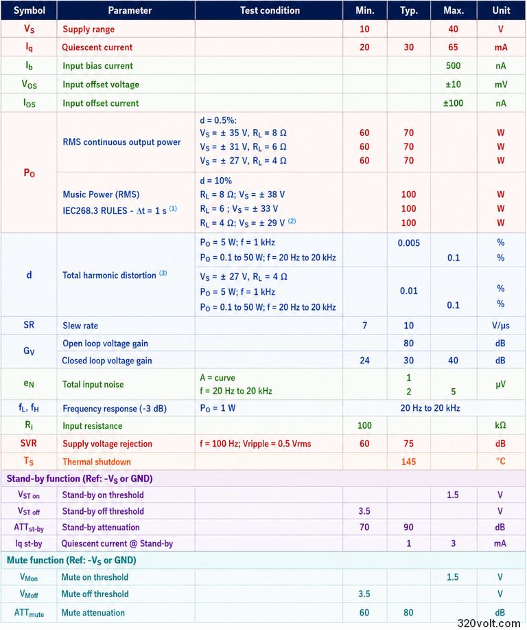
| Feature | Datasheet value | Application note |
|---|---|---|
| IC type | 100 V, 100 W DMOS audio amplifier | Used as a Class AB audio power amplifier. |
| Operating supply range | ±10 V to ±40 V | A symmetrical supply is required; it is not a single-supply circuit. |
| Maximum supply voltage | ±50 V, no-signal condition | The absolute maximum value should not be approached in continuous-operation design. |
| Peak output current | 10 A | Cooling and supply current become critical with low-impedance speakers. |
| Continuous RMS output power | Typical 70 W | Datasheet test value under ±35 V / 8 Ω, ±31 V / 6 Ω, and ±27 V / 4 Ω conditions. |
| Music power | 100 W | Depends on %10 distortion and short-term 1 kHz test conditions; it should not be evaluated like continuous RMS. |
| Closed-loop gain | Typical 30 dB | Set by the R2 and R3 values in the datasheet circuit. |
| Input resistance | 100 kΩ | It is easy to drive from a pre-stage, tone control, or filter circuit. |
| Slew rate | Typical 10 V/µs | Provides sufficiently fast output change for the audio frequency band. |
| Thermal shutdown | 145 °C mute, 150 °C stand-by | Insufficient cooling first mutes the sound, then puts the IC into standby. |
Pin Structure and Functions
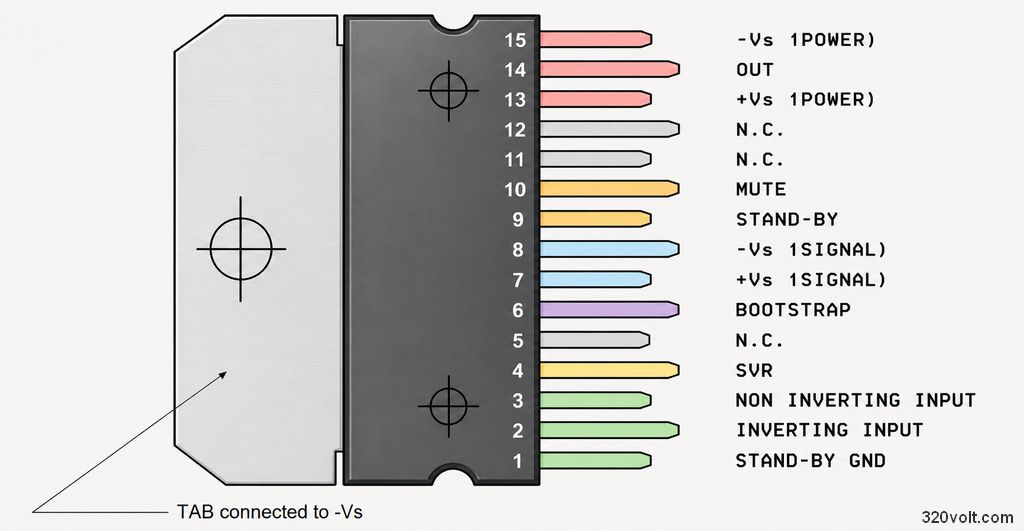
The TDA7294 pinout is given in the Multiwatt15 package. The metal tab connected to the heatsink is connected to the -Vs line.
This point must not be overlooked during assembly; if it will directly contact the chassis or heatsink, an insulating washer and suitable thermal interface material should be used.
| Pin | Name | Function |
|---|---|---|
| 1 | Stand-by GND | Reference connection of the stand-by control circuit. |
| 2 | Inverting input | The inverting input to which the feedback signal is applied. |
| 3 | Non-inverting input | The non-inverting input to which the audio signal is applied. |
| 4 | SVR | Related to supply voltage rejection and the internal reference structure. |
| 5 | N.C. | Unconnected pin. |
| 6 | Bootstrap | Connected to the bootstrap capacitor for the upper drive section of the output stage. |
| 7 | +Vs signal | Positive supply pin of the signal stage. |
| 8 | -Vs signal | Negative supply pin of the signal stage. |
| 9 | Stand-by | Standby control input. |
| 10 | Mute | Mute control input. |
| 11 | N.C. | Unconnected pin. |
| 12 | N.C. | Unconnected pin. |
| 13 | +Vs power | Positive supply pin of the power stage. |
| 14 | Output | Speaker output pin. |
| 15 | -Vs power | Negative supply pin of the power stage. |
Operating Principle of the TDA7294 Typical Application Circuit
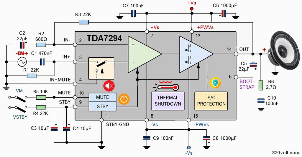
The basic connection in the datasheet uses the TDA7294 as a non-inverting amplifier.
The audio signal enters pin 3 through C1, and the feedback taken from the output is carried to pin 2 through the R3 and R2 network.
This structure keeps the input impedance high while determining the gain in a stable way.
Input and Feedback Network
R1 is the input resistor and is selected as 22 kΩ in the datasheet circuit. C1 blocks the DC component at the input.
The 22 kΩ and 470 nF pair prevents unnecessary DC shift at the lower side of the audio band while ensuring that low frequencies are not completely cut off.
For gain adjustment, R2 is 680 Ω and R3 is 22 kΩ. In a non-inverting amplifier connection, the approximate gain can be considered as GV ≈ 1 + R3/R2.
This value corresponds to approximately 33 times voltage gain, that is, around 30 dB. If the gain is reduced too much, stability may deteriorate; if it is increased too much, input noise and distortion become more visible.
Supply Filtering and Bypass Capacitors
C6 and C8 are 1000 µF capacitors that handle large current pulses on the supply line. C7 and C9 should be placed close to the supply pins of the IC as 100 nF high-frequency bypass capacitors. Large electrolytic capacitors provide current reserve, while small film or ceramic capacitors lower the impedance of the supply line during fast transitions.
In power amplifiers, the supply is not only about the voltage value. The transformer, rectifier, filter capacitor, cable cross-section, and chassis grounding must be evaluated together. Detailed calculation notes on amplifier power supplies are also useful for TDA7294 projects.
Mute and Stand-by Control
Pin 9 is the stand-by control input, and pin 10 is the mute control input. According to the datasheet values, around 1.5 V on these pins is considered the active cutoff region, while above 3.5 V is considered the operating region. The values of R4, R5, C3, and C4 determine the turn-on and turn-off timing.
If C3 and C4 are selected too small, the circuit turns on and off quickly; this may create a pop sound in the speaker. In the sequence recommended by the datasheet, first stand-by is disabled, then mute is disabled. During shutdown, the reverse order is applied. It is possible to manage mute and stand-by with a single control signal, but the time constants must be preserved.
Output Stage and Optional Boucherot Network
The speaker is driven through pin 14. In the datasheet circuit, the R6 2.7 Ω and C10 100 nF network connected to the output is shown as a Boucherot cell. The note states that this network is generally not required in normal stable operation, but it may be needed especially with certain load impedances and supply conditions below ±25 V.
When a long speaker cable, complex crossover structure, or capacitive-type load is used, output stability should be tested more carefully. Using a suitable-power resistive load instead of a speaker at first startup makes it safer to observe faults such as oscillation or DC leakage.
Supply Voltage, Speaker Impedance, and Power Expectation
The TDA7294 datasheet gives different supply conditions for 4 Ω, 6 Ω, and 8 Ω loads. With an 8 Ω speaker, approximately 70 W typical RMS output is possible with ±35 V. With a 4 Ω load, the same power level is delivered with a lower supply voltage, around ±27 V, because output current and heating increase faster.
The 100 W statement is often misinterpreted. The 100 W music power in the datasheet is given under %10 distortion and short-term test conditions. In Hi-Fi applications where clean sound is desired, the value that should be considered is low-distortion continuous RMS power.
For car amplifier or subwoofer applications, a DC-DC converter is required for the TDA7294’s symmetrical supply requirement. In examples aimed at generating a symmetrical supply from 12 V systems, the 12V-28V DC-DC converter structure with IR2153 is one of the typical approaches used in TDA7294 and TDA7293-based projects.
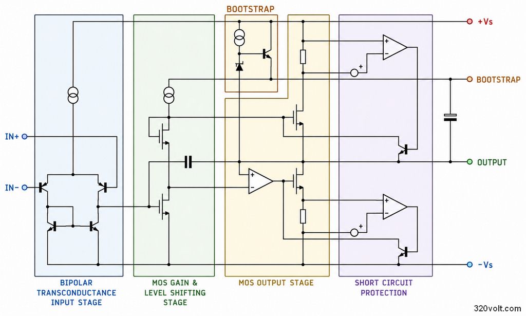
Cooling and Protection Structure
The TDA7294 includes short-circuit protection, SOA protection, and thermal shutdown. These protections do not make the IC completely immune to damage during incorrect use; they only reduce the risk of damage in limit conditions. If a 4 Ω speaker, high supply, and long-term high volume are used at the same time, heatsink size becomes decisive.
In the datasheet, the junction-case thermal resistance is given as 1.5 °C/W. This value is only the heat path from inside the IC to the package. The thermal pad, mica, silicone insulator from the package to the heatsink, and the thermal resistance of the heatsink to air must also be added to the total calculation.
Warning: TDA7294 projects may include symmetrical supplies such as ±35 V, large filter capacitors, and high speaker currents. Before testing, it should be ensured that the capacitors are discharged, and a series lamp or current-limited laboratory supply should be used at first startup.
How Does the TDA7294 Thermal Protection Work?
The TDA7294 includes two-stage thermal protection. When the internal temperature of the IC, that is, the junction temperature, reaches approximately 145 °C, the circuit first enters mute state and the output sound is cut off. If cooling remains insufficient and the temperature rises to approximately 150 °C, the IC is taken into stand-by mode. This behavior protects the speaker and the IC against sudden overheating; however, entering thermal protection continuously indicates that the heatsink is too small, the supply voltage is too high, or the speaker impedance is selected too low.
TDA7294 V Multiwatt15 (Vertical) Mechanical Data
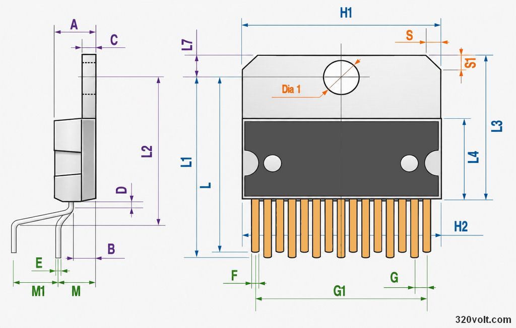
| Dim. | mm | ||
|---|---|---|---|
| Min. | Typ. | Max. | |
| A | 5 | ||
| B | 2.65 | ||
| C | 1.6 | ||
| D | 1 | ||
| E | 0.49 | 0.55 | |
| F | 0.66 | 0.75 | |
| G | 1.02 | 1.27 | 1.52 |
| G1 | 17.53 | 17.78 | 18.03 |
| H1 | 19.6 | ||
| H2 | 20.2 | ||
| L | 21.9 | 22.2 | 22.5 |
| L1 | 21.7 | 22.1 | 22.5 |
| L2 | 17.65 | 18.1 | |
| L3 | 17.25 | 17.5 | 17.75 |
| L4 | 10.3 | 10.7 | 10.9 |
| L7 | 2.65 | 2.9 | |
| M | 4.25 | 4.55 | 4.85 |
| M1 | 4.63 | 5.08 | 5.53 |
| S | 1.9 | 2.6 | |
| S1 | 1.9 | 2.6 | |
| Diam. 1 | 3.65 | 3.85 | |
“`
TDA7294 H Multiwatt15 (Horizontal) Mechanical Data
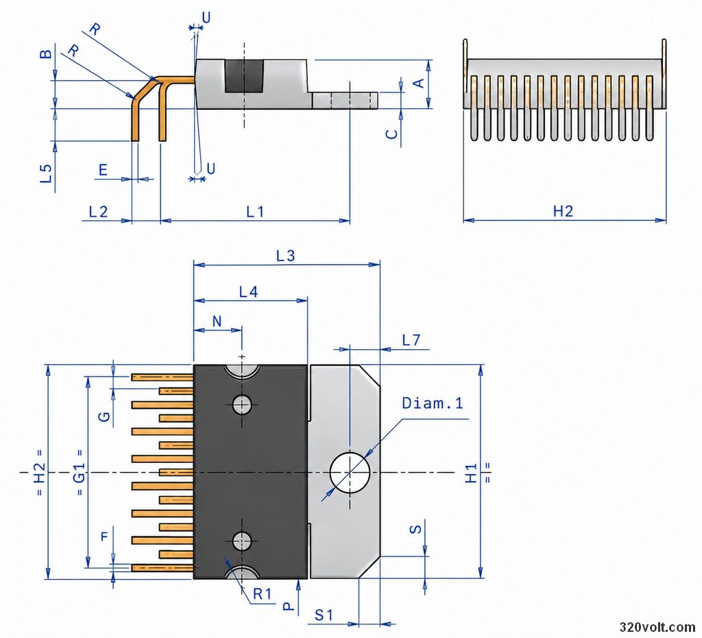
| Dim. | mm | ||
|---|---|---|---|
| Min. | Typ. | Max. | |
| A | 5.00 | ||
| B | 2.65 | ||
| C | 1.60 | ||
| E | 0.49 | 0.55 | |
| F | 0.66 | 0.75 | |
| G | 1.02 | 1.27 | 1.52 |
| G1 | 17.53 | 17.78 | 18.03 |
| H1 | 19.60 | 20.20 | |
| H2 | 19.60 | 20.20 | |
| L1 | 17.80 | 18.0 | 18.20 |
| L2 | 2.30 | 2.50 | 2.80 |
| L3 | 17.25 | 17.50 | 17.75 |
| L4 | 10.3 | 10.70 | 10.90 |
| L5 | 2.70 | 3.00 | 3.30 |
| L7 | 2.65 | 2.90 | |
| R | 1.50 | ||
| S | 1.90 | 2.60 | |
| S1 | 1.90 | 2.60 | |
| Diam. 1 | 3.65 | 3.85 | |
“`
Bridge Connection and Subwoofer Use
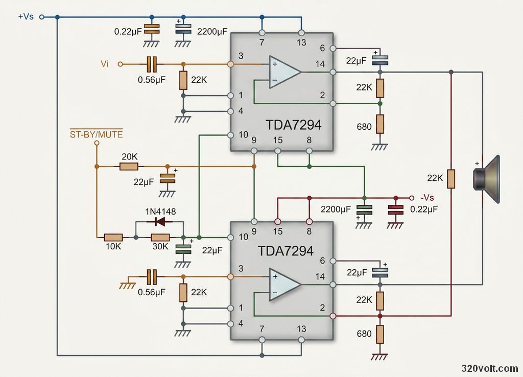
The datasheet shows that two TDA7294 ICs can be used in bridge connection.
In a bridge circuit, two amplifiers operate in opposite phase and the speaker is connected between the two outputs.
In this way, a higher voltage swing occurs across the speaker with the same supply voltage.
In bridge connection, the load impedance should not fall below 8 Ω.
Bridge connection with a 4 Ω speaker causes each IC to see a heavier current load and thermal limits can be exceeded quickly.
Although the bridge structure is attractive for subwoofer applications, the heatsink, supply, and speaker impedance should be selected together.
For practical subwoofer examples with the TDA7294, TDA7294 subwoofer amplifier and TDA7294 100W car subwoofer amplifier projects for vehicle systems can be examined.
In such circuits, the current capacity of the supply converter determines the result as much as the amplifier.
Functions of External Components
| Component | Recommended value | Function | What happens if the value changes? |
|---|---|---|---|
| R1 | 22 kΩ | Input resistor | If it increases, input impedance increases; if it decreases, the previous stage is loaded more. |
| R2 | 680 Ω | Closed-loop gain adjustment | If it increases, gain decreases; if it decreases, gain increases. |
| R3 | 22 kΩ | Feedback from output to inverting input | If it increases, gain increases; if it decreases, gain decreases. |
| R4 | 22 kΩ | Stand-by time constant | Timing changes; very fast transitions may increase pop noise. |
| R5 | 10 kΩ | Mute time constant | Affects mute turn-on/turn-off time. |
| C1 | 470 nF | Input DC isolation | If it decreases, low-frequency cutoff rises. |
| C2 | 22 µF | Feedback DC isolation | Affects low-frequency gain behavior. |
| C3, C4 | 10 µF | Mute and stand-by delay | Small values may cause fast but noisy startup. |
| C5 | 22 µF | Bootstrap capacitor | It affects low frequency and output swing. |
| C6, C8 | 1000 µF | Supply filtering | Insufficient value may cause bass drop, hum, or instability. |
| C7, C9 | 100 nF | High-frequency bypass | Remote placement or omission increases the risk of oscillation. |
Setup and First Test Recommendations
- Long-term power testing should not be performed without attaching the IC to a heatsink.
- Since the metal tab is connected to the -Vs line, heatsink insulation should be checked with a measuring instrument.
- In the first test, a suitable-power 4 Ω or 8 Ω load resistor should be used instead of a speaker.
- Before applying the supply, a short-circuit check should be made between the output and chassis.
- Before connecting the speaker, DC voltage should be measured at the output; if there is high DC, the connection should be disconnected.
- The input cable should be shielded, and the signal chassis should be carried separately from the path where the power current flows.
- Supply capacitors should be placed close to the power pins of the IC.
If a speaker protection relay will be used, startup delay, DC protection, and shutdown behavior should also be considered.
For a more comprehensive stereo or tone-controlled structure, the TDA7294 stereo tone-controlled amplifier with speaker protection project is a good reference point.
Common Mistakes
| Mistake | Possible result | Check point |
|---|---|---|
| Using an insufficient heatsink | Sound cutoff, entering thermal protection, or IC damage | Heatsink temperature, insulating washer, and thermal contact should be checked. |
| Forcing a 4 Ω speaker at high supply | Excessive current and high power dissipation | The supply voltage should be selected according to speaker impedance. |
| Placing bypass capacitors far away | Oscillation, heating, or distorted sound | 100 nF capacitors should be close to the supply pins. |
| Leaving mute/stand-by pins floating | The circuit may not start or may operate unstably | Pin 9 and pin 10 should be driven according to the datasheet thresholds. |
| Forgetting the tab connection | -Vs potential appears on the heatsink | Heatsink insulation and chassis connection must definitely be measured. |
| Connecting input chassis to power chassis at the wrong point | Hum and background noise | Star grounding and short return paths should be preferred. |
In Which Projects Should It Be Preferred?
The TDA7294 is a reasonable choice for applications such as home active speakers, a powerful desktop amplifier, an 8 Ω subwoofer driver, TV or multimedia speaker amplifier.
Thanks to its compact structure, a powerful Class AB output stage can be built without dealing with separate driver transistors.
In multi-channel systems, ready-made audio projects, or comparisons with different ICs, it is also useful to look at an integrated audio amplifier circuits archive.
When selecting the TDA7294, not only the power value, but also speaker impedance, enclosure ventilation, supply transformer, and protection circuit should be evaluated together.
Equivalent and Selection Notes
The datasheet does not provide a direct equivalent list for the TDA7294. Therefore, if another IC will be selected, the pinout, supply limit, mute/stand-by thresholds, package structure, and heatsink connection should be checked one by one.
TDA7293 or different TDA series ICs may be seen in similar applications; however, direct replacement without checking the schematic is not safe.
Counterfeit or low-quality ICs often cause problems in high-power amplifier circuits.
Testing with low supply, current limiting, and a load resistor at first startup protects both the speaker and the power supply.
TDA7294 Datasheet: You can examine the STMicroelectronics TDA7294 datasheet PDF file.