The light switch-off delay circuit is a 230V AC compatible MOSFET timer that keeps the LED lamp on for a short time after the wall switch is turned off. It is suitable for experienced users who want delayed lighting of approximately 50-90 seconds in corridors, entrances, and passage areas.
Main Purpose of the Circuit
Contents
- 1 Main Purpose of the Circuit
- 2 Connection Logic
- 3 Circuit Schematic and Block Structure
- 4 Technical Specifications
- 5 Component List
- 6 How Does the Circuit Work?
- 7 Why Is Load Selection Important?
- 8 Points to Pay Attention to During Assembly
- 9 MOSFET Selection
- 10 Safety Warnings
- 11 Common Problems
- 12 Where Can It Be Used?
- 13 Limits of the Circuit
In a classic wall switch, the lamp turns off completely as soon as the contact opens. This can create the need for a few extra seconds of lighting, especially in corridors, stair landings, entrances, or around an outside door.
The timer circuit is connected in parallel with the existing switch connection and allows current to pass for a certain time after the lamp is turned off.
This system does not use a continuously timed relay like a staircase timer. When the switch is closed, the circuit is almost outside the system.
When the switch is opened, the module becomes active, powers the lamp for a while longer, and cuts the voltage when the delay is completed.
Connection Logic
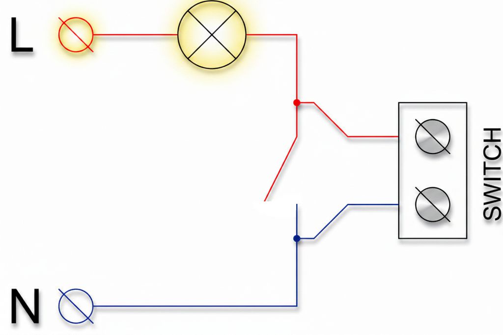
The circuit is connected in parallel to the two contacts of the wall switch. Therefore, it is not necessary to bring the entire phase and neutral line to the module; the module uses the voltage between the two ends of the switch.
When the switch is closed, the two ends are short-circuited and no meaningful voltage is formed across the module.
When the switch is opened, mains voltage appears at the module terminals because of the line coming through the lamp.
At this moment, the delay circuit starts operating and continues to pass current to the lamp through the IRF830 MOSFET.
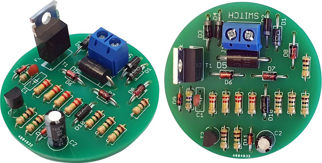
Circuit Schematic and Block Structure
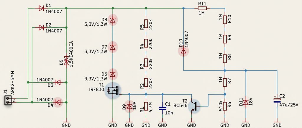
No microcontroller or timer IC is used in the schematic. The delay time is created with high-value resistors, the C2 capacitor, and the T2 transistor.
The main current carrying the lamp passes through the D1-D4 diodes and the T1 IRF830 MOSFET.
D1-D4 Bridge Rectifier Section
The D1, D2, D3, and D4 diodes work like a bridge rectifier so that the MOSFET can be used on the AC line.
IRF830 is an N-channel MOSFET controlled in one direction. The mains voltage, however, is alternating current.
The diode bridge makes the current direction on the MOSFET side unidirectional, allowing T1 to control the AC load.
This method is a practical solution for delayed turn-off of low-power LED lamps without using a triac.
The holding current problem that can be seen in triacs is less noticeable here; with low-power LED loads, the MOSFET behaves more flexibly.
T1 IRF830 Power Switch
T1 IRF830 is the switching component of the circuit. After the switch is opened, the lamp current continues to flow through T1.
Since IRF830 is a high-voltage N-channel MOSFET, it is in a class that can be used in a 230V AC application.
When the MOSFET is conducting, the voltage going to the lamp is slightly lower than the mains voltage. In the circuit, a voltage of around approximately 10V is left across the D6, D7, and D8 zener diodes.
Since most LED lamps have an internal driver circuit, this small drop generally does not disturb operation.
D6-D8 Zener Chain
D6, D7, and D8 are a series chain consisting of three 3.3V zener diodes. This section helps create the voltage required for MOSFET gate control. When the circuit is active, a total voltage of around approximately 10V is formed across this zener chain.
This voltage creates the control energy that keeps T1 on. At the same time, it causes some voltage drop on the load side.
For this reason, the circuit works more compatibly especially with LED lamps that have electronic drivers.
Gate Protection and Filtering
D9 18V zener diode limits the gate-source voltage of the T1 MOSFET.
MOSFET gate terminals are sensitive to high-voltage spikes; exceeding the permitted value can easily damage the component. Therefore, D9 is a critical protection component.
R2, R3, R4, and R5 resistors limit the current in the gate control line.
The use of these resistors in series is not only to increase the total resistance value; it also divides the voltage falling across each resistor on the 230V line and prevents a single component from being overstressed.
The C1 10nF capacitor smooths the ripple on the rectified voltage.
The R1 4.7M resistor helps discharge C1 and the MOSFET gate-source capacitance.
Turn-Off at the End of the Delay with T2 BC546
The delayed turn-off section of the circuit is built around the T2 BC546 transistor. The C2 capacitor slowly charges through the R8, R9, R10, and R11 resistors.
As the C2 voltage rises, the voltage reaching the base of T2 increases.
When a certain threshold is exceeded, T2 conducts and discharges the gate-source of the T1 MOSFET with low impedance.
Since the gate voltage disappears, T1 turns off. Thus, the lamp can no longer receive current and turns off.
C2 Timing Capacitor
The C2 47uF/25V capacitor is the most important component that determines the delay time.
Since the capacitor is slowly charged through high-value resistors, a delay on the order of seconds is obtained.
The delay time should not be considered like a fixed laboratory timer.
The power of the LED lamp, the current passing through the zener diodes, ambient temperature, and component tolerances affect the time.
The same circuit may give a longer delay with a 2W LED lamp and a shorter delay with a 20W lamp.
Function of D10 and D11
The D11 18V zener diode prevents the C2 capacitor from being charged with excessive voltage. Since the operating voltage of C2 is 25V, this limitation is important.
The D10 1N4007 diode helps C2 discharge faster when the switch is closed again.
If the switch is opened again before C2 is fully discharged, the delay time may be shorter than normal. Therefore, the time may change in rapid consecutive on-off tests.
Technical Specifications
| Feature | Value / Description |
|---|---|
| Operating voltage | 230V AC / 50Hz |
| Connection type | Parallel to wall switch contacts |
| Delay time | Approximately 50-90 seconds |
| Load range | Approximately 2-30W |
| Recommended load | LED lamp |
| Switching component | IRF830 N-channel MOSFET |
| Delay component | C2 47uF capacitor and high-value resistor chain |
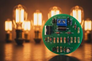
| PCB size | Round board approximately 48 mm in diameter |
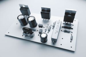
Component List
| Reference | Value / Model | Function |
|---|---|---|
| R1 | 4.7MΩ | Helps discharge C1 and the MOSFET gate capacitance. |
| R2-R5 | 220KΩ | Limits current in the gate supply line and distributes high voltage across the resistors. |
| R6 | 510KΩ | Part of the divider and discharge path for the T2 base voltage. |
| R7-R11 | 1MΩ | Determine the C2 charging time and delay behavior. |
| C1 | 10nF MKT | Filters the rectified voltage on the MOSFET gate line. |
| C2 | 47uF / 25V | The timing capacitor that creates the delay time. |
| D1-D4 | 1N4007 | The AC line is rectified for the MOSFET. |
| D5 | 1.5KE400CA | Provides protection against high-voltage spikes. |
| D6-D8 | 3.3V / 1.3W zener | Creates an approximately 10V reference for MOSFET gate control. |
| D9 | 18V zener | Limits the MOSFET gate-source voltage. |
| D10 | 1N4007 | Helps the C2 capacitor discharge quickly. |
| D11 | 18V zener | Limits the maximum voltage across C2. |
| T1 | IRF830 | High-voltage MOSFET that carries the lamp current during the delay time. |
| T2 | BC546 | Turns off the lamp by discharging the T1 gate voltage when the time expires. |
| J1 | 2-pin terminal block | Input point where the module is connected to the wall switch terminals. |
How Does the Circuit Work?
When the Switch Is Closed
When the wall switch is closed, the lamp lights normally. Since the module is connected in parallel to the switch terminals, these two ends are almost short-circuited.
Since sufficient voltage is not formed across the circuit, the timing section does not operate actively.
At this stage, the C2 capacitor must discharge. If the switch is kept closed for a very short time and opened again, C2 may not discharge completely and the next delay time may be shorter than expected.
When the Switch Is Opened
The moment the switch is opened, the lamp should normally turn off. However, the module electronically bridges the switch contacts for a while longer.
The current rectified through the D1-D4 diode bridge is passed by the T1 MOSFET and the LED lamp continues to light.
At the same time, the C2 capacitor begins to charge slowly. This charging process forms the time base of the delay.
When the Time Expires
When the C2 voltage reaches a level that turns on the T2 transistor, T2 discharges the gate-source line of T1.
T1 turns off and the lamp current is cut. According to the application note in the source text, the LED lamp may turn off with an approximately 2-second soft transition at the end of the delay.
Why Is Load Selection Important?
The circuit is especially suitable for LED lamps between 2W and 30W. With low-power LED lamps, the delay time may be longer.
With higher-power LED lamps, since the current through the zener chain increases, C2 charges faster and the time may become shorter.
Incandescent lamps may theoretically work; however, the purpose of the circuit is low-power modern LED lighting.
Behavior should not be assumed in advance with electronic transformer spotlights, smart bulbs, motion-sensor lamps, or special drivers that operate with very low standby current.
Points to Pay Attention to During Assembly
- The circuit operates directly with the 230V AC mains line; it should not be tested exposed.
- Assembly should only be performed by people competent in mains electricity.
- Series resistor chains such as R2-R5 and R8-R11 should not be randomly replaced with a single resistor.
- The polarity of the C2 electrolytic capacitor must be connected correctly.
- The directions of D6-D8, D9, and D11 zener diodes should be checked carefully.
- The PCB should be used inside an insulated enclosure or junction box so that it does not touch conductive surfaces.
- Terminal connections should not be left loose, and cable ends should not remain exposed.
MOSFET Selection
In the schematic, IRF830 is used for T1. If an equivalent is to be selected, an N-channel, high-voltage MOSFET in a TO-220 package should be preferred.
The drain-source voltage rating should be at least around 500V, and the on-channel resistance should not exceed a few ohms.
Since the switched power in this circuit is low, a modern MOSFET with a very low RDS(on) value is not mandatory.
Nevertheless, using a low-quality MOSFET or a MOSFET with insufficient voltage rating may lead to failure during mains spikes.
Safety Warnings
This circuit is not an isolated low-voltage circuit. The entire board should be considered to be at mains potential.
If measurement is to be made, an isolation transformer, suitable probe, insulated working surface, and experienced measurement method are required.
Do not touch the board, lamp, switch terminals, or terminal blocks while the circuit is operating.
After power is cut, wait for the capacitors to discharge, and then verify by measurement.
It is not a suitable application for beginners.
Common Problems
| Symptom | Possible Cause | Check Point |
|---|---|---|
| The lamp turns off without any delay | T1 may not be conducting or the gate control line may not be working. | D6-D8, D9, R2-R5, and T1 connections should be checked. |
| The delay is too short | C2 may not have discharged completely, or the lamp power may be shortening the time. | A test should be performed after the switch has remained closed for at least 1 minute. |
| The lamp never turns off | T2 may not be able to discharge the gate line. | The area around T2, C2, R6, R7, and D11 should be examined. |
| The LED lamp flickers | The lamp driver may be incompatible with this series MOSFET structure. | A different brand or a more suitable power LED lamp should be tried. |
| The time changes when the circuit operates again | The C2 capacitor has not fully discharged from the previous cycle. | D10 and the R6-R7 discharge line should be checked. |
Where Can It Be Used?
- Leaving the corridor lamp on for a short time after turning it off
- Being able to see the keyhole after turning off the switch at an outside door or garage entrance
- Providing temporary lighting until reaching the other switch at a stair landing
- Obtaining delayed turn-off in short-term passage areas such as storage rooms, pantries, or entrances
Limits of the Circuit
The timing value is not precise. The delay range of approximately 50-90 seconds may vary depending on the application.
This circuit should be considered as a practical delayed turn-off solution rather than a time relay adjusted to exact seconds.
Also, since the circuit is powered through the load, it may not give the same result with all LED lamps.
Testing may be required with very low-power, smart-controlled, or complex-driver lamps.
For safety, the module must definitely be used inside a closed and insulated enclosure.
Source: ep.com.pl/projekty/projekty-ep/16598-opozniacz-wylaczenia-swiatla