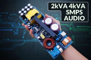
The 0-1200 V adjustable flyback SMPS circuit is a 120 W class power supply designed to obtain isolated high voltage from the mains. Its output can be controlled with a PWM signal, it can charge capacitive loads, and it is a design example worth examining for experienced electronics users working with high-voltage experiments.
Basic Purpose of the Circuit
Contents
- 1 Basic Purpose of the Circuit
- 2 Why Was the Flyback Topology Chosen?
- 3 Technical Specification Summary
- 4 Input Stage and Mains Rectification
- 5 Primary Switching Stage
- 6 Why Is Transformer Design Critical?
- 7 Secondary Rectification and 6-Section Output Structure
- 8 Control Circuit and Use of UCC38C45
- 9 Current Limiting and Short-Circuit Behavior
- 10 Voltage Regulation and Stability
- 11 Why Is a Discharge Circuit Necessary?
- 12 Notes for Setup and First Test
- 13 Common Mistakes
- 14 Safety Warning
- 15 Evaluation
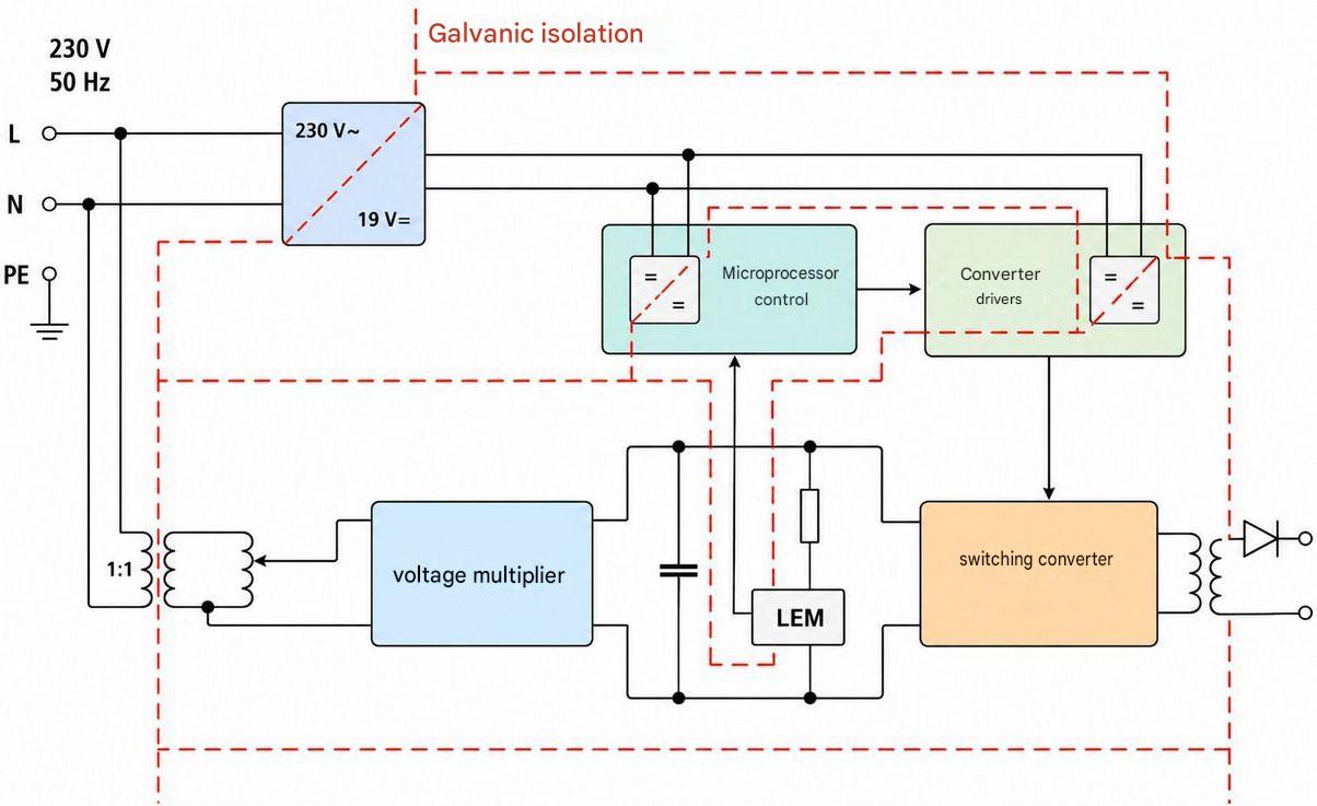
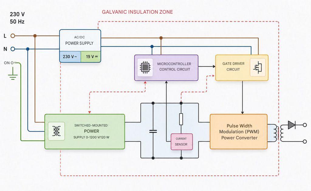
The purpose of this design is to create an isolated high-voltage power supply powered from the 230 V AC mains, with an output adjustable in the range of approximately 0-1200 V and capable of delivering power at the 120 W level.
The circuit is described as a high-voltage source developed to supply the intermediate circuit capacitors of an irreversible electroporation device.
In high-voltage sources, simply increasing the voltage is not sufficient.
The output must be galvanically isolated from the mains, the current must be limited during a short circuit or empty capacitor charging, the switching component must be protected against voltage spikes, and feedback stability must be ensured.
Therefore, the circuit should be handled much more carefully than a simple boost converter.
Why Was the Flyback Topology Chosen?
A blocking converter, that is, flyback topology, is used in the design. This choice is especially reasonable in applications requiring high voltage and relatively low output current.
In a flyback structure, energy is stored in the magnetic field of the transformer while the switch is conducting; when the switch turns off, this energy is transferred to the output capacitors through the diodes on the secondary side.
The advantages of the flyback structure for this project are as follows:
- It can operate with a single switching component.
- It provides isolation between the mains and the output.
- The secondary turns ratio can be easily adjusted to generate high output voltage.
- It does not require a separate filter inductor at the output.
- It is suitable for applications requiring pulsed energy transfer, such as capacitive load charging.
On the disadvantage side, leakage inductance can create high-voltage spikes on the primary switch. Therefore, PCB layout, snubber structure, IGBT selection, and transformer winding arrangement directly affect reliability.
For basic information about flyback and SMPS structures, the topic of switching power supplies can also be examined.
Technical Specification Summary
| Feature | Value / Description |
|---|---|
| Input | 230 V AC mains |
| Output voltage | Adjustable high voltage in the 0-1200 V range |
| Output power | Approximately 120 W |
| Topology | Isolated flyback / blocking converter |
| Switching frequency | 30-40 kHz operating range |
| Control structure | UCC38C45 / UC3845 family current-mode PWM control |
| Main power component | 1200 V class SGP07N120 IGBT |
| Output structure | High-voltage rectification and capacitor structure divided into 6 sections |
| Auxiliary supply | ±15 V control supply |
Input Stage and Mains Rectification
At the input of the circuit, the 230 V AC mains voltage is rectified to obtain a high-voltage DC intermediate bus.
This section includes the bridge rectifier, filter capacitors, input protection components, and connections important for EMI.
When the mains is rectified, a dangerous level of DC voltage occurs across the capacitors; therefore, only a suitable probe, isolation transformer, and safe discharge method should be used during measurement.
The X2 and Y2 class capacitors in the input filter should not be selected randomly.
If the appropriate safety class is not used for capacitors connected directly to the mains, leakage, heating, or explosion risk may occur during a fault.
Limiting components such as an NTC or series resistor are also used to reduce the sudden capacitor charging current at the moment of first power-up.
Primary Switching Stage

On the primary side, a 1200 V class SGP07N120 IGBT is used as the main switching component. Although the MOSFET option is common in high-frequency SMPS circuits, in MOSFETs above 600 V, conduction resistance and switching behavior often become disadvantageous. Therefore, in this design requiring 1200 V voltage withstand capability, an IGBT has been a more suitable choice.
In a flyback converter, while the switch is conducting, current rises through the primary winding and energy is stored in the core. When the switch turns off, the primary current is reset, the diodes on the secondary side conduct, and the stored energy is transferred to the output capacitors. During this time, not only the rectified mains voltage but also the voltage reflected from the secondary and spikes caused by leakage inductance appear across the primary switch.
Therefore, the current loop around the IGBT should be kept short. If the conductive paths between the primary capacitor, switch, transformer primary, and protection components are long, leakage inductance increases. As a result, higher voltage peaks, more heating, and unstable operation may be seen on the IGBT.
Why Is Transformer Design Critical?

In a high-voltage flyback SMPS circuit, the task of the transformer is not only to provide a voltage ratio.
The transformer is also an energy storage component. Primary inductance, air gap, core cross-section, maximum flux density, and winding arrangement directly determine the output power.
An ETD59 class ferrite core is used for the main pulse transformer in the SMPS design.
The primary winding was calculated as 40 turns, and the secondary side was divided into 6 separate sections to increase high-voltage withstand capability and reduce diode voltage stress.
A segmented secondary winding provides a more controlled structure in terms of insulation and rectification compared to a single-piece high-voltage winding.
Winding Arrangement and Leakage Capacitance
The secondary winding producing very high voltage makes interwinding capacitance important. If the parasitic capacitance between the primary and secondary becomes large, switching pulses can be carried to the control circuit and measurement lines. In the project, it is stated that parasitic transformer capacitance caused serious problems during the commissioning process.
In this type of supply, winding the transformer only according to the number of turns calculation is not sufficient. The layer order of the windings, insulation tape, winding start and finish directions, primary-secondary distance, and shielding decision should be evaluated together. Especially at outputs above 1000 V, standard low-voltage SMPS experience alone is not sufficient.
For those working on transformer calculation and core selection, the basic formulas on the power electronics calculations page may also be useful.
Secondary Rectification and 6-Section Output Structure
On the secondary side, the output is not taken through a single diode and a single capacitor. Instead, the secondary winding is divided into 6 sections, and each section is arranged to operate with its own rectifier diode and capacitor. This method reduces the reverse voltage to which the diodes are exposed and makes high-voltage insulation more manageable.
In each section, the capacitor charges to approximately one sixth of the total output voltage. At 1200 V output, this value is approximately around 200 V per section. When the secondary winding voltage and capacitor voltage are considered together, diode selection should still have high-speed operation and sufficient reverse voltage withstand capability.
Slow-recovery diodes can cause serious losses and voltage spikes in flyback circuits. Not only the current and reverse voltage rating of the diode, but also its reverse recovery time should be checked. For general diode behavior, the operating principle of diodes can be a basic reference.
Control Circuit and Use of UCC38C45
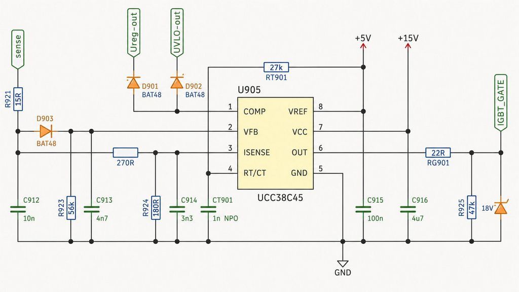
On the control side, the UCC38C45 / UC3845 family current-mode PWM control structure is used. In current-mode control, the primary current is monitored in every switching cycle.
When the current reaches the set limit, the PWM pulse is terminated. This method provides more controlled behavior, especially in demanding situations such as short circuit and capacitive load charging in flyback converters.
For voltage regulation, the output voltage is divided and measured, then transferred to the control circuit as feedback.
In the high-voltage measurement divider, the total voltage rating, power dissipation, and insulation distance of the resistors are important.
Using suitable voltage-rated resistors connected in series instead of a single resistor is safer.
For more general information about the PWM controller IC family, the article on the UC3843 SMPS PWM controller IC can also be examined.
UC3843 and UC3845 do not have exactly the same operating limits; however, they can be evaluated within the same family in terms of current-mode PWM control logic.
Current Limiting and Short-Circuit Behavior
Since the output of the high-voltage power supply will charge large capacitors, a behavior similar to a short circuit may occur at the first moment.
An empty capacitor appears like a low-impedance load at the moment it is first connected to the supply. Therefore, current limiting in the design is not only fault protection, but also part of normal operating behavior.
A low-value shunt resistor is used for primary current sensing. The voltage across the shunt is applied to the current-sense input of the PWM controller IC.
This signal must be filtered so that parasitic pulses do not cause false triggering; however, if the filter is too slow, real overcurrent is detected late.
This balance is one of the most sensitive points of flyback SMPS design.
Voltage Regulation and Stability
It is stated that oscillation was observed in the output voltage and regulator output during the first tests of the circuit. This is a common problem in high-voltage supplies.
The output capacitor, feedback divider, optocoupler or isolation circuit, and PWM controller IC together form a closed loop.
If this loop is not properly compensated, the supply may operate unstably even in the no-load condition.
It is observed that the output voltage ripple decreases when a capacitive load is connected. The reason for this is that the large capacitor suppresses low-frequency voltage changes. However, simply adding a large capacitor to the output is not a permanent solution; regulator compensation, current limit, and discharge circuit should be adjusted together.
Why Is a Discharge Circuit Necessary?
Capacitors charged up to the 1200 V level can retain dangerous energy even after power is cut.
Therefore, the circuit includes a discharge structure that discharges the output capacitors in a controlled way.
If the discharge resistor is selected as directly and continuously connected, it causes unnecessary power loss; a switched or controlled discharge structure can be more efficient.
The power rating of the discharge resistor should be calculated carefully. A resistor selected for short-term discharge may overheat if it is continuously activated due to regulation oscillation.

Notes for Setup and First Test
It is not the correct method to connect and test an SMPS circuit of this class directly to the mains.
In the first test, the control supply, PWM output, gate drive signal, shunt voltage, and feedback line should be checked separately.
Before the power stage is activated, it should be verified that the PWM signal maximum duty limit, current sensing threshold, and whether the pulse is cut off in case of a fault operate correctly.
For first power-up, a series lamp, isolation transformer, current-limited variac, or suitable laboratory test setup should be used.
Using a ground-referenced probe on the mains-connected primary side during oscilloscope measurements is very dangerous. A differential probe or isolated measurement method should be preferred.
Points That Should Be Checked
- It should be checked whether there is excessive noise after the pulse on the primary shunt signal.
- The IGBT collector-emitter voltage should not peak above the expected limits.
- The gate drive signal should have sufficient amplitude and clean edges.
- The secondary diodes should be monitored in terms of heating and reverse recovery.
- The voltage rating of the resistors in the output voltage divider should be sufficient.
- The transformer insulation should be suitable for high-voltage testing.
- The output capacitors should be safely discharged after power is cut.
Common Mistakes
| Mistake | Possible Result |
|---|---|
| Carrying the primary current loop with long PCB traces | High-voltage peaks and EMI problems occur on the IGBT. |
| Using a secondary diode with insufficient reverse recovery characteristics | The diode heats up, loss increases, and the output waveform deteriorates. |
| Using low-voltage resistors in the feedback divider | Breakdown or measurement error may occur across the resistor. |
| Neglecting insulation distance in transformer winding | Leakage or high-voltage arcing may occur between primary and secondary. |
| Selecting the current sensing filter too slow | The switch is overstressed during short circuit or capacitor charging. |
| Trying to discharge the output capacitors by hand | Risk of electric shock and arcing occurs. |
Safety Warning
This circuit operates with mains voltage and can produce DC voltage above 1000 V at its output.
Such a supply carries the risk of serious electric shock, arcing, fire, and measurement equipment damage even at low current.
If an experimental setup will be built, isolation, fuse, grounding, creepage distances, capacitor discharge, and closed enclosure must definitely be part of the design.
It is not suitable to build the circuit on a breadboard. Sufficient creepage and clearance distances should be left between high-voltage lines, sharp-pointed copper areas should not be used on the PCB, and output terminals should be protected against touch.
Before making measurements, it should be verified that the capacitors are discharged.
Evaluation
The 0-1200 V adjustable flyback SMPS design provides a good application example for those who want to develop a high-voltage power supply.
Topology selection, transformer winding, IGBT stress, secondary segmentation, current-mode control, and regulation stability are considered together in the circuit.
Nevertheless, this design should not be seen as a simple hobby circuit to be copied directly.
The most critical points are transformer insulation, primary leakage inductance, secondary diode selection, feedback stability, and safe test method.
Without checking these topics, a high-voltage SMPS circuit will not operate reliably.
Source: dspace.vut.cz/items/d57eaa04-d9e7-4942-9220-4fdb19046682