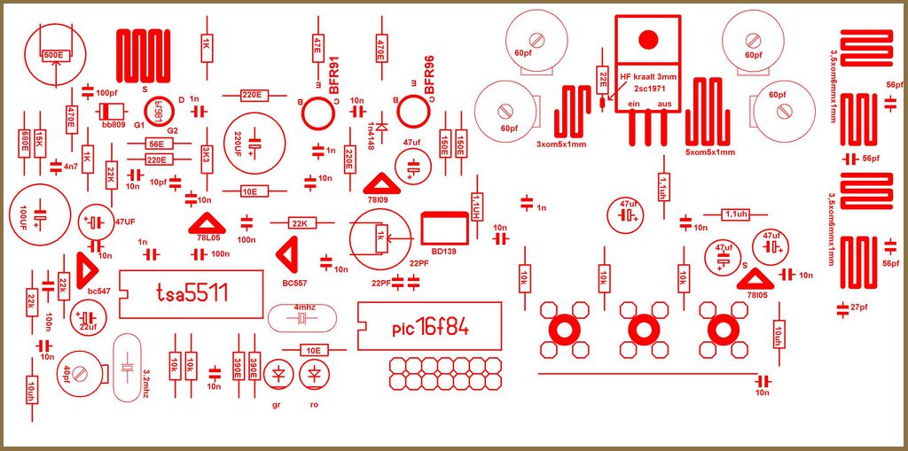
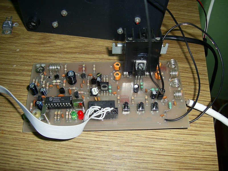
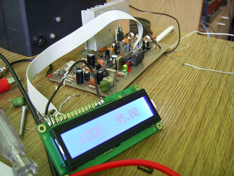
PLL FM 8W transmitter circuit is an RF project board with digitally adjustable frequency in the 88-108 MHz band, controlled by a TSA5511 PLL synthesizer and PIC16F84. The circuit uses a BF981 oscillator, BFR91/BFR96 intermediate RF stages, a 2SC1971 output transistor, a 1×16 LCD display, and three-button frequency control together.
A forgotten project in the archive… I do not know where it came from, but I had noted the following comment;
A very nicely working PLL modulator. I built it myself and got very clean sound. Some foreign sites mention that it gives 8 watt output, but I think in the worst case around 7 watt output is obtained. If you are really curious, you can build it. If you have a little PIC knowledge, you will not encounter any problems. The points you need to pay attention to are the 3.2mhz crystal and a properly programmed PIC16F84.
Since the 3.200Mhz crystal connected to the pin of the TSA5511 is the reference crystal, it must be exactly 3.200mhz. You should also make fine adjustment with the adjustable capacitor next to it. If you can make a proper adjustment, you may observe a 200hz drift between maximum frequencies.
If you adjust it at every frequency you set, you may observe a drift between 10-20hz. It is an extremely nice circuit. Its version is 2004 V1, and as far as I have observed, newer versions have also been released. I will try to share them with you very soon. New versions 2006v6 and v7 have been released. SMD components were used in v7, so I think it will be even more precise.
General Structure of the Circuit
Contents
- 1 General Structure of the Circuit
- 2 How Do PLL and Frequency Control Work?
- 3 RF Amplifier and 2SC1971 Output Stage
- 4 Power Supply Stage and Voltage Notes
- 5 LCD and 14 Pin Box Header Connection
- 6 Points to Consider During Assembly and Testing
- 7 RF Shielding and Enclosure Use
- 8 Technical Summary
- 9 Legal and Technical Responsibility
- 10 Project Difficulty Level
Unlike simple FM transmitters with a classic free-running oscillator, the board has a more stable structure that locks the frequency with PLL.
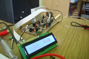
Frequency adjustment is done with the UP, DOWN, and SET buttons; the selected value is shown on the 1×16 character LCD display.
According to the markings on the PCB, the supply voltage is 13.8V, and the operating range is designed as the 88-108 MHz band.
In this type of project, phase-locked loop and frequency synthesizer PLL logic is important for understanding the PLL section. Because the stability of the transmitter depends not only on the oscillator circuit, but also on how properly the oscillator is locked by the PLL.
| Section | Main component used | Function |
|---|---|---|
| Oscillator / VCO | BF981, BB809 | The section where the RF carrier signal is generated and its frequency is changed with a varicap diode. |
| PLL control | TSA5511 | Compares the oscillator frequency with the reference and ensures that the frequency remains locked. |
| Microcontroller | PIC16F84 | Reads the buttons, controls the PLL IC, and sends frequency information to the LCD display. |
| RF amplifier | BFR91, BFR96 | Amplifies the low-level RF signal at the VCO output to a level suitable for the power stage. |
| Output stage | 2SC1971 | The final transistor stage that provides RF output power. |
| Power supply | 7805, 78L05 | Provides 5V regulation for digital control and low-voltage sections. |
How Do PLL and Frequency Control Work?
The basis of frequency generation in the circuit is the RF oscillator section built with BF981. The BB809 varicap diode allows the oscillator frequency to be controlled.
The TSA5511 PLL IC monitors this oscillator frequency and generates a control voltage according to the value set by the PIC16F84.
Thus, the frequency remains more stable against factors such as hand proximity or temperature changes compared to free-running VFO circuits.
Three buttons are used on the PIC16F84 side: UP, DOWN, and SET. According to the explanation in the source file, the frequency can be changed in the 88-108 MHz range with 0.05 MHz steps.
For similar LCD-controlled PLL structures, the PLL FM transmitter with LCD display using PIC16F627A and TSA5511 can also be considered in the same project family.
Crystal/resonator components marked as 4 MHz and 3.2 MHz can be seen on the PCB. The 4 MHz component may have been used for the clock source on the PIC side, and the 3.2 MHz component for the PLL reference structure.
Without the complete schematic, the connection of these two oscillator components should not be stated definitively; the original values on the PCB should be preserved during assembly.
RF Amplifier and 2SC1971 Output Stage
The RF signal at the VCO output is not at a level that can be fed directly to the antenna. For this reason, intermediate amplification is first done with BFR91 and then BFR96 on the board; in the final stage, the 2SC1971 RF power transistor is used.
The 2SC1971 is an RF power transistor used in the VHF band, and it can easily be damaged in case of incorrect load, poor cooling, or incorrect adjustment.
In the output section, there is a filter/matching network formed with coils, trimmer capacitors, and small-value RF capacitors.
Values such as 56pF, 60pF, and 27pF on the PCB, together with the coil dimensions, show that this stage is designed for the VHF band.
For those interested in RF power stages, the RF amplifier, PLL, RDVV, encoder, and receiver-transmitter circuit archive is directly related to this project.
Why Is the Output Filter Critical?
In an FM transmitter circuit, it is not enough for only the fundamental frequency to be strong. The output stage can also produce harmonic components.
Therefore, the output filter is important both for spectrum cleanliness and for making the connected antenna appear as the correct load to the power stage.
For this reason, the spacing of the filter coils, the adjustment of the trimmers, and the short RF paths on the PCB should not be changed randomly.
For a simpler approach using a similar band, a comparison can be made with a simple 88-108 MHz FM transmitter circuit. This 8W PLL design, however, is a more difficult project for beginners because of its higher power, PLL locking, and LCD-controlled operation.
Power Supply Stage and Voltage Notes
There is a 13.8V supply marking on the board. This value is a common nominal supply level in automotive electronics and radio/RF equipment.
7805 and 78L05 regulators are used for the digital control and LCD section. Electrolytic capacitors should be selected with a voltage rating of at least 16V or higher.
Since the RF power stage may draw current, a current-limited power supply should be used during initial startup. The 2SC1971 output transistor should not be stressed without a heatsink or when an antenna/dummy load is not connected.
Applying reverse polarity to the supply line of the circuit can cause permanent failure in the PIC, TSA5511, and RF transistors.
LCD and 14 Pin Box Header Connection
A 1×16 character LCD display is used in the project. The display connection is provided through a 14-pin box header. LCD pin 15 is specified as the backlight positive end, and pin 16 as the negative end to be connected to chassis/ground. The notes also state that an extra wire should be drawn from the LCD pin 2 or pin 3 connection to the common supply of the buttons.
| 14 pin connector | PIC16F84(A) | LCD / Button connection |
|---|---|---|
| 1 | 9 | LCD pin 14 |
| 2 | 10 | LCD pin 4 |
| 3 | 8 | LCD pin 13 |
| 4 | 11 | Down button |
| 5 | 7 | LCD pin 12 |
| 6 | 12 | Set button |
| 7 | 6 | LCD pin 11 |
| 8 | 13 | Up button |
| 9 | 5 / GND | LCD pin 5 |
| 10 | 5 / GND | LCD pin 1 |
| 11 | 4, 14 / +5V | LCD pin 2 |
| 12 | 4, 14 / +5V | LCD pin 3 |
| 13 | 2 | LCD pin 6 |
| 14 | 1 | LCD pin 15, LCD pin 16 chassis/ground |
Points to Consider During Assembly and Testing
This board is not a circuit that can be assembled like a simple single-transistor transmitter and tested with a random antenna.
The RF stages must see the correct load, the output filter must be adjusted, and the PLL lock must operate properly.
For those who want to start with lower-power examples, projects such as a 500mW FM PLL transmitter may be a more suitable intermediate step.
- A 50 ohm dummy load with suitable power rating should be used instead of an antenna during the first test.
- The supply current should be limited; if the current suddenly increases, the circuit should be turned off and the output stage should be checked.
- 2SC1971 cooling should not be neglected, and the transistor should not be operated unloaded for a long time.
- Coil spacing and trimmers should not be turned randomly; adjustment should be made with RF measurement equipment.
- When making the LCD connection, pin 1 direction and box header order should be checked twice.
- The RF section should preferably be shielded with metal compartments; the oscillator, driver, and output filter should be separated from each other.
- If the audio input will be provided from a computer or external source, the level should be started low.
RF Shielding and Enclosure Use
One of the practical points emphasized in the forum notes is shielding. In the VHF band, even a conductive path of a few centimeters can create unwanted coupling.
If the oscillator section, intermediate amplifier, and output filter are placed in separate compartments inside the same metal enclosure, stability increases.
If the power transformer will be placed in the same enclosure, it should be kept away from the RF section and shielded against magnetic field coupling.
Antenna, height, and environmental conditions greatly change the range. Although it is stated in the source project that a long-distance test was performed with a dipole antenna, this value is not guaranteed.
Those interested in this topic can examine long-distance FM transmitter projects only for technical comparison purposes.
Technical Summary
| Feature | Value / Description |
|---|---|
| Circuit type | PLL-controlled FM transmitter |
| Frequency range | 88-108 MHz |
| Frequency step | 0.05 MHz |
| Supply | 13.8V DC |
| Control IC | TSA5511 PLL synthesizer |
| Microcontroller | PIC16F84 / PIC16F84A |
| Display | 1×16 character LCD |
| RF oscillator | BF981 and BB809 varicap structure |
| RF intermediate stages | BFR91 and BFR96 |
| Output transistor | 2SC1971 |
| Software file | rdvv.hex is provided as the PIC program file |
Legal and Technical Responsibility
The 88-108 MHz band is the broadcast band, and unauthorized RF broadcasting is illegal in many countries. This project should be evaluated for educational and laboratory examination purposes.
Instead of open-antenna transmission tests, an attenuator load, shielded test enclosure, and suitable RF measurement equipment should be used.
For the frequency to appear clean, not only PLL lock but also the output filter and harmonic measurement should be checked.
Project Difficulty Level
The 8W PLL FM transmitter circuit is not considered a beginner project for those without RF measurement experience. PCB production, mechanical precision of the coils, PLL lock, output filter, power transistor cooling, and legal limitations should be considered together. Learning low-power transmitter and PLL logic first, then moving on to this type of RDVV-based board, is a safer path.
source: elektroda.pl/rtvforum/topic1288529.html