The 6 Watt FM RF amplifier circuit with 2SC1971 is a VHF power stage designed to increase the output of low-power transmitters operating in the 87.5-108 MHz FM band. With approximately 300 mW RF input, correct adjustment, and a suitable 50 ohm load, approximately 6 W output is targeted. PCB layout, cooling, and output tuning are as important as the circuit schematic in this project.
Basic Technical Specifications of the Circuit
Contents
| Feature | Value / Description |
|---|---|
| Operating band | FM broadcast band, 87.5-108 MHz |
| RF input power | Approximately 300 mW |
| RF output power | Approximately 6 W with proper adjustment and load |
| Supply | 12 V DC |
| Power transistor | 2SC1971 RF power transistor |
| PCB structure | Double-sided FR-4, microstrip-line design |
| PCB size | 77 x 56 mm |
| SMD components | 1206 package |
| Input / output connection | BNC connector, suitable connection for 50 ohm RF line |
Operating Principle of the Circuit
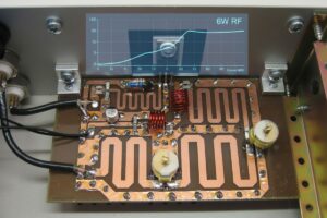
2SC1971 6 Watt FM RF amplifier circuit schematic

The circuit operates as a single-transistor VHF RF power amplifier. The low-power RF signal at the input is applied to the base of the 2SC1971 transistor with suitable impedance.
The signal amplified on the collector side is transferred to the RF output through the output matching network consisting of microstrip lines and adjustable capacitors.
RF Input Stage
The RF signal at approximately 300 mW level coming from the BNC connector at the input is carried to the base region of the transistor through 220 pF capacitors and the inductive trace on the PCB.
The 22 pF, 47 pF, 1 µH, and 56 ohm components help shape the input impedance and RF return path.
In the VHF band, the length of the input line, capacitor leads, and soldering quality can change the circuit behavior.
Therefore, component placement is as important as the electrical connection in the schematic.
Long cables, unnecessary jumpers, or high-inductance connections can reduce the gain of this stage or make the circuit unstable.
2SC1971 Power Transistor
The 2SC1971 transistor is used in the power stage. This transistor is an NPN RF transistor used in VHF RF power applications.
In the schematic, the emitter is connected directly to the ground line; the base is driven with the RF signal, and the collector is connected both to the supply line and to the output matching network.
The body of the 2SC1971 must be firmly mounted on a heatsink. Thermal paste should be used, and no air gap should remain between the transistor and the heatsink.
If the heatsink selection is insufficient, the transistor may overheat in a short time even if output power is obtained. A heatsink with a thermal resistance around 6 °C/W or lower should be preferred.
Mounting the 2SC1971 RF power transistor on the heatsink

Collector Supply and Decoupling
On the collector side, the 5-turn coil is used together with 1 nF, 100 nF, and 22 µF/25 V capacitors to keep the supply line clean in terms of RF.
The purpose here is to deliver the DC supply to the transistor while reducing RF energy leakage into the supply cable.
Using only a high-capacitance electrolytic capacitor on the supply line is not sufficient.
At around 100 MHz, the placement of small-value ceramic capacitors becomes more critical.
The 1 nF and 100 nF capacitors should be kept close to the transistor, and their ground connections should be short and made with a wide surface.
Output Matching Network
The RF energy taken from the collector is not fed directly to the output connector.
Between them, there is a matching network consisting of PCB inductors, 1.2 nF capacitors, and 70 pF adjustable capacitors.
This section brings the collector impedance of the transistor closer to the 50 ohm output line.
The output network, which operates with fixed capacitors in the original layout, has been made more practical here with adjustable capacitors.
When the operating frequency in the FM band changes, trimmer capacitors provide an important advantage so that the output stage can be adjusted for the highest efficiency.
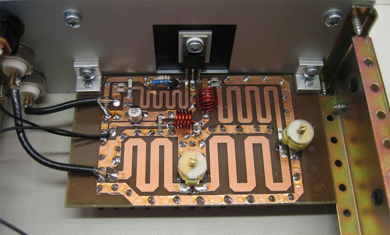
In-enclosure assembly of the 6 Watt RF amplifier and adjustable capacitors
Critical Points in PCB Design
This circuit is not a simple RF circuit that can be transferred onto perforated phenolic board.
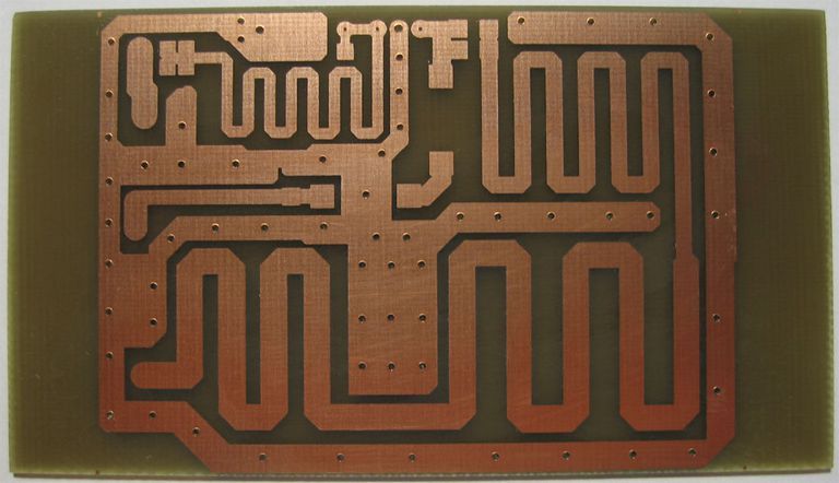
The copper traces on the PCB, especially the microstrip lines on the output side, operate as part of the circuit.
If the trace width, board size, or print scale changes, the inductance and impedance values also change.
Top-side PCB microstrip traces of the 6 Watt RF amplifier
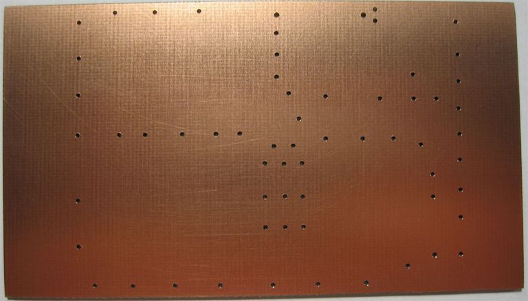
The bottom surface is left as a wide ground plane. The ground regions on the top surface and the ground plane on the bottom surface must be connected to each other with many vias.
If these connections are neglected, the RF return current circulates through unwanted paths; gain may decrease, output adjustment may become difficult, or the amplifier may oscillate.
Bottom-surface ground plane of the 6 Watt RF amplifier
No scale error should be made during PCB production. The file was prepared at 600 dpi resolution and 77 x 56 mm size.
If automatic fit, fit-to-page, or a different scale is selected while printing, the behavior of the microstrip lines changes.
In home production, PCB fabrication requires special attention to double-sided alignment and via connections.
Component and Coil Notes
| Component / Section | Value | Function |
|---|---|---|
| Input capacitors | 2 x 220 pF | RF input coupling and input matching network |
| Input-stage capacitors | 22 pF, 47 pF | Shapes the RF impedance on the base side |
| Input shunt coil | 1 µH | RF return path and input-stage impedance arrangement |
| Base-side resistor | 56 ohm | Helps damping and stability in the input stage |
| Power transistor | 2SC1971 | RF power amplification component |
| Collector coil | 5 turns, 0.8 mm enameled copper wire, 6.4 mm inner diameter | RF component between the collector and the supply/matching stage |
| Supply decoupling | 1 nF, 100 nF, 22 µF/25 V | Suppresses RF components on the supply line |
| Output capacitors | 2 x 1.2 nF | RF coupling and matching on the collector output side |
| Adjustable capacitors | 2 x 70 pF | Adjustment of the output stage according to the operating frequency |
| PCB inductors | Microstrip traces on the board | Inductive components of the output matching network |
The diameter of the enameled copper wire used in the coils is important. In the notes, 1.0 mm wire is given as approximately AWG18, 0.8 mm wire as approximately AWG20, and 0.3 mm wire as approximately AWG28.
The coil diameter should be evaluated by the inner diameter, not the outer diameter. The 6.4 mm inner diameter should be maintained for the 5-turn coil.
Points to Consider During Assembly
All SMD components are soldered directly to the top surface of the PCB.
In the RF stage, leaving long leads, moving components with wires, or placing trimmer capacitors away from the board is not suitable.
Especially the connections of the 70 pF adjustable capacitors should be short, and they should not move mechanically during adjustment.
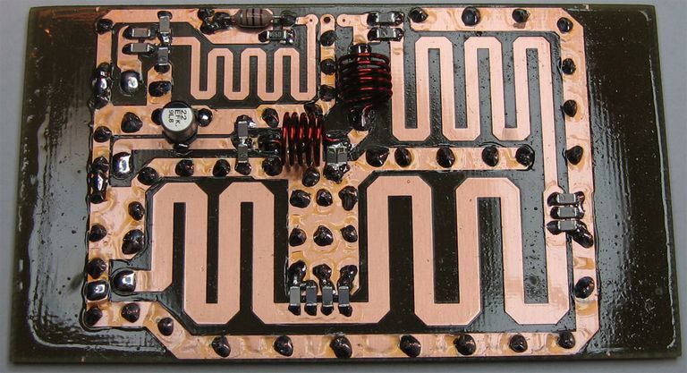
Component-assembled PCB of the 6 Watt FM RF amplifier
- The bottom ground plane and the ground points on the top surface must be connected with many vias.
- The 2SC1971 body must be tightly fixed to the heatsink.
- The supply cable should be kept short and routed away from the input and output RF cables.
- The chassis connection of the input and output BNC connectors should have a wide surface.
- Adjustable capacitors should be selected from types suitable for operation in the VHF band.
- Care should be taken that the transistor is not counterfeit or a low-quality equivalent.
In RF power circuits, soldering quality is more effective than it appears.
A cold solder joint or cracked via connection may not be noticed at low frequency; around 100 MHz, however, it can noticeably reduce the output power.
First Startup and Adjustment
In the first test, a suitable-power 50 ohm dummy load should be connected to the output instead of an antenna.
If an RF wattmeter is available, output power and reflected power should be monitored together.
If an RF wattmeter is not available, a suitable-power small bulb can be used temporarily for rough adjustment, but this method does not provide precise impedance measurement.
- First, connect the 12 V supply without applying RF input and check whether there is excessive current.
- The circuit must not be operated without connecting a 50 ohm dummy load to the output.
- The FM exciter is started at low power, and the input level is increased slowly.
- After the operating frequency is selected, the 70 pF adjustable capacitors are adjusted for maximum output and low reflection.
- The transistor temperature is monitored during adjustment.
- Before long-term operation, the output spectrum and harmonics should be checked.
The approximately 300 mW input level is the value specified for this design. Driving it harder may lead the transistor to saturation, heating, and unwanted harmonics instead of making it more powerful.
With lower input, the output power naturally decreases. In similar RF applications, the cooling and impedance-matching logic in RF power amplifier designs for different power levels can also be compared.
Enclosure, Panel, and Connections
In the enclosure design, the rear panel includes the 12 V DC input, RF input, and RF output connections.
In the images, BNC connectors are used for input and output. On the front panel, there is an on/off switch, power LED, and “6 Watt RF Amplifier” label.
Rear panel of the 6 Watt RF amplifier with 12V DC RF input and RF output connectors

Front Panel Designer was used for the panel drawings. Source .fpd files are available. When preparing similar aluminum front panel work, the switch, LED, BNC, and DC socket holes can be aligned more neatly with a panel design program.
The chassis connection inside the enclosure also affects RF performance. The BNC bodies, PCB ground plane, and metal enclosure should be connected to each other with the lowest possible impedance.
A chassis connection made with only a thin wire may not be sufficient in the VHF band.
Common Mistakes
| Mistake | Possible Result |
|---|---|
| Printing the PCB at the wrong scale | The impedance of the microstrip lines changes, and the output tuning does not hold |
| Not connecting the bottom and top ground surfaces sufficiently | Unstable operation, low gain, or oscillation may occur |
| Testing the transistor without a heatsink | The 2SC1971 may overheat in a short time |
| Operating the output without a load | Reflected power may damage the transistor |
| Adjusting the trimmer capacitors randomly | Output power decreases and harmonics may increase |
| Using long connection cables | Input/output matching is disturbed and the circuit becomes frequency-sensitive |
Legal and Technical Safety Notes
Amplifying RF power in the FM band may require legal authorization. Although the circuit is technically prepared to operate in the 87.5-108 MHz band, connecting it to an antenna and transmitting is subject to restrictions depending on the country and purpose of use. A dummy load should be used in laboratory tests, and unauthorized transmission should not be performed.
Looking only at the power level at the RF output is not sufficient. Harmonics, spurious emissions, and antenna mismatch must also be checked.
If suitable equipment is not available, at least the output should be tested at low power, and the circuit should be adjusted indoors with a dummy load instead of a real antenna.
When working with FM transmitter projects, the output level, modulation, and filtering topics on the FM transmitter side should also be evaluated together.
This 6 Watt FM RF amplifier made with the 2SC1971 is a project with high layout sensitivity despite its simple component count.
As much as the component values in the schematic, the double-sided structure of the PCB, via connections, microstrip-line dimensions, transistor cooling, and output adjustment determine the result.
For those without VHF experience, the safest method is to first test on a dummy load with low input power and adjust the output in a controlled way.
Source: bygselvhifi.dk/projects/6-watt-rf-amplifier/