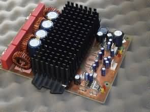
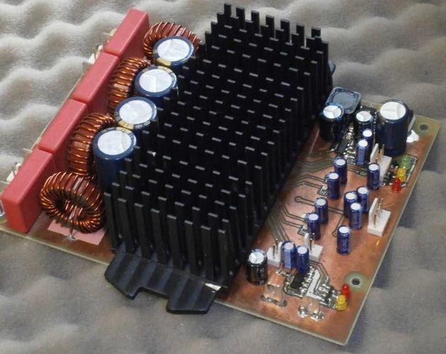
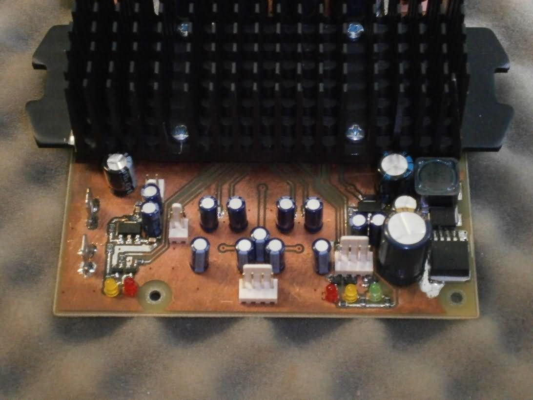
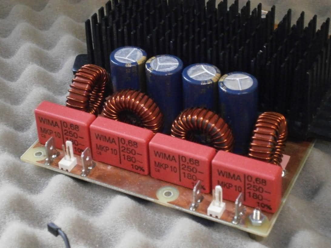
The core of the whole amplifier circuit is the TAS5630B one connection is based on modified the recommended BTL mode stereo input, which is listed by the manufacturer in Selection of the final chip involvement consisted of four different modes, of the optional input pins M1 to M3:
TAS5630B 2 x BTL – two separate channels (full bridge connection, power up to 2x300W)
TAS5630B 1 x PBTL – the only channel in bridging (parallel output up to 1x400W)
TAS5630B 4 x – four separate channels (performance 4x145W to 2? Or 4x75W into 4?)
TAS5630B 1 x BTL + 2 x SE – two channels involved in half the bridge (SE) and one channel to full bridge (BTL), suitable, for example, for 2.1 speakers. Selected was mode 2 x BTL, I mean the classic stereo modes,
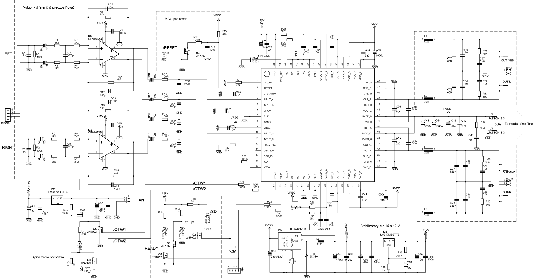
TAS5630B from which it can be seen that the input the signal is transferred to the pins of INPUT_A to D, which then goes into the filter slucky. In this block processes the input signal together with the signal from the feedback then progressing through the analog multiplexer to the analog comparator, where PWM modulation occurs by comparing the input signal and the signal from the oscillator, which is known from the theory of the D-class block of the PWM receiver Process the PWM signal and oversees its parameters through the feedback of the slug through the detector the activities of PWM.
Block TAS5630B protection circuit supervises the block management on the end transistors that it is possible to disconnect the short circuiting or crossing the temperature of the chip. The following block management is the timing, which is responsible for the correct timing and switching for terminal transistors and thus can not occur to the current opening in the counter phase (the so-called “dead time”). For this block, followed by the actual drive, powered from pins GVDD_A to D and behind them are the power terminal transistors, which power supply is transferred through the pins PVDD_A to D. The outputs of the end transistors are then out to the pins of OUT_A to D.
TAS5630B circuit schematic
![]()
FILE DOWNLOAD LINK LIST (in TXT format): LINKS-26175.zip

AVR-ISP MKII Programmer Circuit
AVR-ISP MKII Programmer Circuit
AVR microcontrollers are most commonly used for AVR-ISP MKII programmer programming with serial interface ISP. They are cheap and uncomplicated. However, these programmers have lost their versatility because Atmel has introduced new microcontrollers, programmed with PDI and TPI interfaces. The programmer presented in the article is universal, it will be useful to both older and newer AVRs.
This programmer is compatible with AVR-ISP mk.II and allows programming of all 8-bit AVR microcontrollers via ISP, PDI and TPI interfaces. It works with the latest version of AVR Studio (which can be downloaded for free from the AVR website), ImageCraft and Codevision AVR compilers.
Its heart is the AT90USB162 microcontroller clocked with a 16 MHz quartz resonator X1. The programmer power is downloaded from the USB connector of the PC. The USB interface can also be powered by a programmable circuit, which enables the jumper JP1.
List of AVR microcontrollers depending on the type of programming interface
On the output side, the AVR-ISP MKII programmer has a special buffer by which it is possible to program microcontrollers fed with different voltages, whereby the programmable microcontroller can be energized by the programmer or the voltage of the programmed system. Choosing the supply voltage enables the jumper. The programmer communicates with the computer using the USB interface. The computer can run under Windows XP, Vista, 7.
Circuit d’amplification de classe D TAS5630B 300W
Le cœur de tout le circuit de l’amplificateur est le TAS5630B, une connexion est basée sur l’entrée stéréo recommandée en mode BTL, qui est répertoriée par le fabricant dans la sélection de l’implication finale de la puce composée de quatre modes différents, des broches d’entrée optionnelles M1 à M3 :
TAS5630B 2 x BTL – deux canaux séparés (connexion pont complet, alimentation jusqu’à 2x300W)
TAS5630B 1 x PBTL – le seul canal en pontage (sortie parallèle jusqu’à 1x400W)
TAS5630B 4 x – quatre canaux séparés (performances 4x145W à 2? Ou 4x75W à 4?)
TAS5630B 1 x BTL + 2 x SE – deux canaux impliqués dans la moitié du pont (SE) et un canal vers le pont complet (BTL), adaptés, par exemple, pour des enceintes 2.1. Le mode 2 x BTL a été sélectionné, je veux dire les modes stéréo classiques,