If the mosfet is built on the amplifier circuit SG3524, the spp80n06 output can be adjusted between 21v…28 volts. The standard output voltage is specified as 24 volts. The output filter coil in the used core pc power supplies is removed from two used AT power supplies, and there is also a proteus ares PCB file.
12V 24V – 10A BOOSTER CONVERTER This converter uses BOOST structure, fixed frequency pulse width modulation (PWM) regulation. Optimized for best performance.
The frequency is fixed between 80 and 100 kHz (non-critical value). A lower frequency requires a higher inductance, which increases the volume and losses. Too high a frequency leads to negligible switching losses in the transistor and additional losses in the inductance due to the skin effect.
In the principle diagram, we see that the main sources of loss are:
The resistance of the inductance is L (we will neglect the iron losses)
The state resistor RDSon of transistor Q (we will neglect the switching losses)
Voltage drop across the diode
Series resistance (ESR) of capacitor C
The choice of these components is therefore decisive.
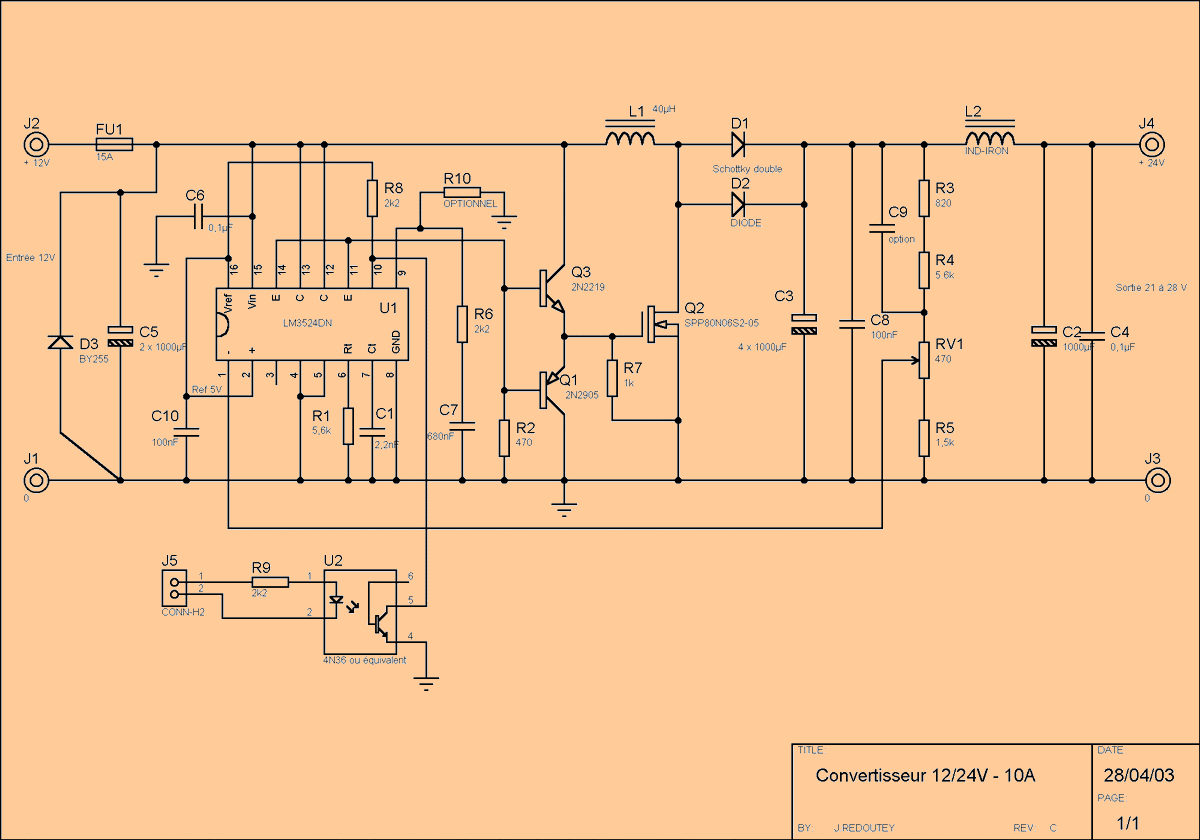
Inductance The value of the inductance affects the ripple of the current passing it, hence the peak current passing other elements. Theoretical work shows that 40 to 50 µH is a good compromise. The inductance intersects with an alternating direct current whose average value is equal to the current consumed in the battery:
Ibat = Output power / battery voltage x efficiency
With a 12V battery, the current consumed is 22.2A with 24V – 10A output and 90% efficiency. If the battery drops to 10V, the current rises to 26.6A.
This current passes the inductance, so it is necessary to ensure that the magnetic material used is not saturated for this current, which increases by half the ripple (peak current).
Recall that the passage of a current I in the N turns of the inductance creates a magnetic excitation H, which results in the material with a certain induction B, which must remain lower than the saturation induction Bsat of the magnetic material under consideration.
Therefore, we should choose a magnetic material with high induction and low losses (mainly with eddy currents). There are special alloys such as molypermalloy that exhibit such properties, but mostly powdered iron toroids are used. The iron powder grains are bound by an insulator, which provides a distributed air gap and increases saturation induction.
I used two iron powder cores with a diameter of 30mm and a thickness of 11mm (yellow cores found in old AT type PC power supplies). Two tori are placed side by side and held together by a round adhesive tape. The number of turns to be wound is about fifteen.
Given the high current flowing through the inductor, a large copper section is required, which is achieved by winding several wires in parallel (easier than winding a single thick wire and better for skin effect, see Litz’s thread).
Proceed as follows:
Prepare 4 lengths of enameled wire with a diameter of 1 mm (cut a little longer…)
Twist the 4 wires together, you can easily do it by attaching one end to a doorknob or vise and crimping the other end with a hand drill. Turn it very tight as the thread then loosens up.
Starting from the middle of the wire, wrap the wire around the bagel, tighten the turns well against the bagel and distribute it around the perimeter.
15 turns in this way. Take an extra turn if the window has some space left. Be careful, what matters is how many times the wire goes through the donut.
Power selection MOSFET transistor.
You should choose a TO220 or TO293 N-channel MOS transistor in plastic packaging that holds at least 45V and has the lowest RDson possible. A good performance-price compromise is Infineon’s SPP80N06S2-05 (available from Radiospares), which receives 55 V and has an RDS (on) rating of 4.8 mW.
Diode selection
It is imperative to use a large-caliber Schottky diode to minimize voltage drop. I used dual TO293 diodes found in PC power supplies or 40CPQ045 from IR (available from Radiospares). Two diodes are connected in parallel.
Capacitor selection
It is imperative to use capacitors with a low ESR (equivalent Series Resistance) because they intersect with a very high effective current. The use of ordinary electrochemical capacitors leads to very strong output voltage fluctuation and overheating. Several capacitors are connected in parallel to achieve a low ESR. I used Rubycon low ESR 1000µF – 35V capacitors (available from Radiospares)
Control circuit
I chose National’s LM3524DN. It is an improved version of the ‘3524’ standard. Other versions of ‘3524’ will not work in this circuit. To use them, it is necessary to make a divider bridge on the reference and change the resistance values of the output bridge.
The LM3524 is equipped with a shutdown input, which allows the Q transistor to be blocked. The converter does not work and the output voltage is equal to the input voltage (minus the voltage drop across the diode). This is useful when powering a PA because the converter can be blocked in reception (no interference) or run at low power to save battery. Implementation is accomplished using a simple photocoupler that offers the advantage of an isolated command.
Additional filtering
An LC cell has been added to the output to provide the cleanest possible voltage. The inductance used is not critical, it just needs to support the output current (recycle in PC power supply).
This type of converter causes a relatively large current increase at opening. Do not use a current-limiting stabilized power supply during tests. Indeed, the supply voltage is crashing, the MOS transistor is poorly controlled and can be destroyed. The supply voltage should not fall below 10V.
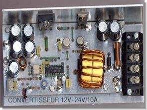
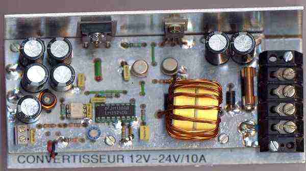
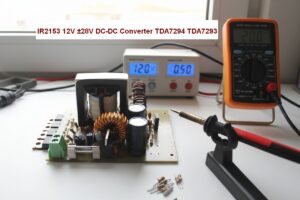
The converter is made on a 130 x 65 mm double-sided printed circuit. The top face is all copper and acts as the ground plane (to connect to the ground rails on the other side).
The transistor and diode are placed on the edge of the board to be mounted on a radiator through an electrical insulator (mica or choterm from a PC power supply), which is a good conductor of heat. Given the low dispersion of these elements, it is useless to provide a large heatsink. bent at right angles and a simple aluminum sheet is sufficient, acting as a support for the assembly.
I inserted a glass cartridge fuse holder into the printed circuit. This does not allow currents above 15A. To use the circuit at its maximum power, connect the fuse holder and connect an appropriately rated automotive fuse in series. First of all, do not bypass the fuse because the circuit is not short-circuit protected.
The reference voltage from the LM3524D is 5V. To get another output voltage, it is enough to change the bridge of the resistors R3, R4, RV1, R5 so that there is 5V on the slider RV1. Be careful, the voltage can get too high and break a component. The circuit is calculated for an adjustable voltage between 21 and 28 V.
The input voltage can vary between 10 and 15 V. Outside of this range there is risk for the MOS transistor.
Source: f6csx.free.fr DC DC Boost Converter Circuit 12V to 24V SG3524 PWM schematic pcb files alternative link:

PIC18F452 examples (asm, c)
PIC18F452 example applications are also available in a variety of information and documents
Assambly Language example
LCD
IR RX
IR TX
LM35 bin
Flash Led
LM35 bcd
Timer0 int
LM35 bcd uart
C Language example
LM35 proje
Sample C project
Flash Led
Hello. Can you advice how to improve this schematic for parallel using for increase of current up to 20a and more?