A lot of people interested in electronics applied a variation of the classic two-transistor flip flop circuit design using 2 different operating states provided the same circuit. LEDs are enabled 6.
first transistor T1 now suppose that the message (D4 -D3 BURN OFF ) . In this case T1 collector voltage will be closer to zero volts, and for the first time would be short-circuited capacitor C1 to bias the base of transistor T2 and T2 will fall will enter into insulation . Capacitor C1 through resistor R3 is the base bias of transistor T2 times of charging will increase relatively .
Increased base bias collector current of T2 while improving at the same time will reduce the collector voltage . Meanwhile, the first moment of the capacitor C2, T1 acts like a short circuit will cut the base bias (D3 -D4 BURN OFF ) . Thereby charging the capacitor C2, the transistor T1 will remain on until the insulation . Transistors in the circuit in order to change this state of isolation from the message and the collector square wave signal at the output will be obtained. In the circuit will operate independently as two -fold career can be controlled only place is designed .
Flip-Flop Circuit isis Simulation

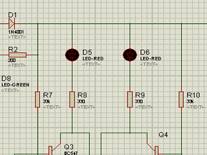
flip flop circuit diagram of the proteus circuit simulation:


BCD Counter 74LS160 Serial Connection Example Circuit
A design of serial connection to the instance of the circuit 74ls160. This can be done by connecting to the desired number, counting up the şekildeö integrated serial. 2 entgre count can be done with 99. 5 integrated with the number 99 999 a removable. 74ls160 integrated circuit oscillator circuit with number 2 connecting the output CLK pin 555 circuit frequency according to the substitution can be made.
74LS160 Example Circuit Serial Connection schematic