The mosfet amplifier was originally made as a subwoofer amplifier, but that doesn’t mean that the amplifier performs poorly in the rest of the frequency range. It’s a powerful, quality amplifier that performs very well in all conditions.
There are 2 dual mosfet versions that work with +-20…45VDC symmetrical voltage and 4 dual mosfet versions that work with +-20…60VDC voltage.
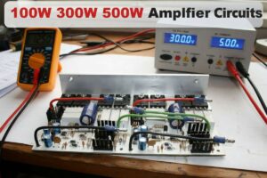
Mosfet Amplifier Specifications (Based on Multisim 14 circuit simulation):
- Frequency response re 1kHz (-1dB) = 4 – 110,000Hz
- Frequency response re 1kHz (-3dB) = 2 – 200,000Hz
- Maximum output power (4 ohm load, 1kHz, +/- 40VDC, driving 2 pairs of output transistors) = 150W
- Maximum output power (4 ohm load, 1kHz, +/- 40VDC, driving 4 pairs of output transistors) = 380W
- THD+N (-1dB from maximum power, 1kHz, 4 ohms) = 0.006%
- Supply voltage range (when driving 2 pairs of output transistors) = +/-25VDC … +/-45VDC
- Supply voltage range (when driving 4 pairs of output transistors) = +/-25VDC … +/-60VDC
First test; the sound was very nice, I felt the difference of the mosfet 🙂 but testing an amplifier with a mosfet without a heatsink is a wrong decision, also the quiescent current was a bit high (80mA) I guess I should have taken the trouble and made the adjustment
A new article will come when it is completed…. let’s continue for now;
The resistors in the amplifier circuit, except for those specified, are 0.25 W. It is better to use metal film resistors because of their lower noise. Attention should be paid to the quality of the capacitors (C1 and C5) included in the signal path. It is better to use a non-polar electrolyte like C5 (can be polar).
Mosfet Amplifier Circuit Diagram

The amplifier operates in class AB and therefore requires quite serious cooling. The qualitative characteristic of the heat sink is its surface area and the thickness of the base. To remove 1 W of heat, about 15 cm2 of heat sink area is required (for aluminum and its alloys). The thickness of the base – the more, the better. The required heat sink area can be calculated using the formula:
S = Pout * (1 – efficiency) * 15, where Pout is the output power of the amplifier. For a 150W amplifier, the minimum heat sink area should be: S = 150 * (1 – 0.6) * 15 = 900 cm. When using active heat dissipation (one fan or more), the heat sink area can be reduced.
The output coil consists of 15-20 turns, the wire cross-section is 1-1.5 mm2, the diameter is 8 mm. The accuracy of the coil is not of great importance.
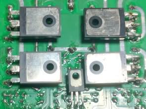
The output power of the amplifier depends primarily on the amplifier supply voltage. With two pairs of output transistors, it is strongly recommended not to exceed the supply voltage +/-45V (with 4-8 ohm speaker resistance). The output power limit with two pairs of transistors is 150W. When using four pairs of output transistors, the supply voltage can be increased to +/- 60V, the output power will be 380W at 4 ohm load.


Connection points on the board:
IN: Audio signal input.
sGND: Audio input ground (ground from signal source).
OUT: Amplifier output.
GND: One contact to connect to the ground of the power supply, the second to the negative output of the amplifier to the speaker.
+/-V: To connect the amplifier power supply.
There are 5 different PCB drawings of the Mosfet amplifier. The first original version I implemented. I added a pot and made a few adjustments. Also, a multi-turn trimpot was added to the 750-ohm resistor for the quiescent current.

source: cxem.net/sound/amps/amp206.php