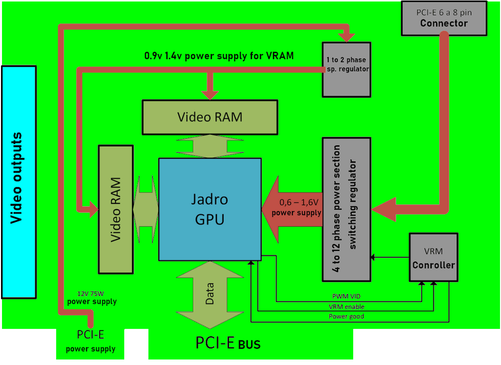
Design and implementation of a low voltage and high current multi-phase switching power supply to be used for computer graphics card repair. Graphics Card Repair The features of the power supply are 150A minimum output current, an output voltage ranging from 0.9 to 1.5V adjustable or set to a fixed level using PWM VID, and fully passive, pcb cooled.
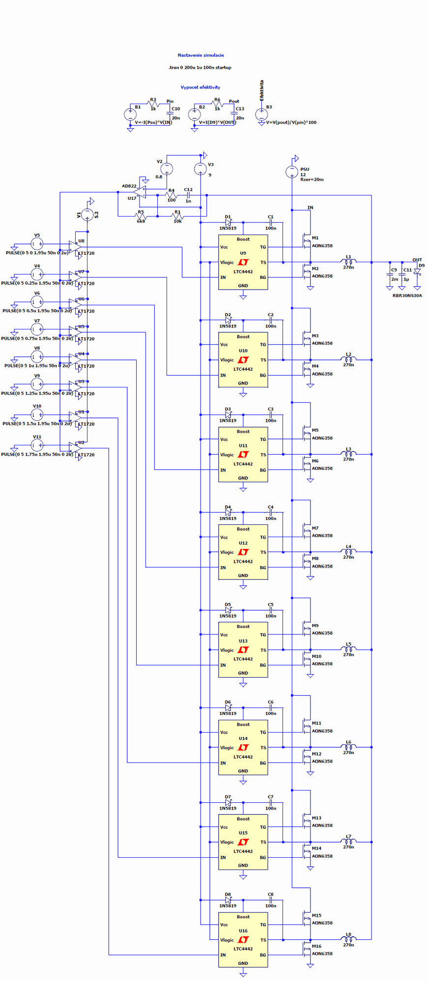
A Multi-Phase Synchronous-Buck Control integrated circuit, uP9511, is used for PWM control. The power stage uses a SiC789 integrated circuit that can provide up to 60A continuous current per phase. There are Eagle cad 9.6.2 schematics, pcb drawings and Ltspice files for the DC-DC converter project.
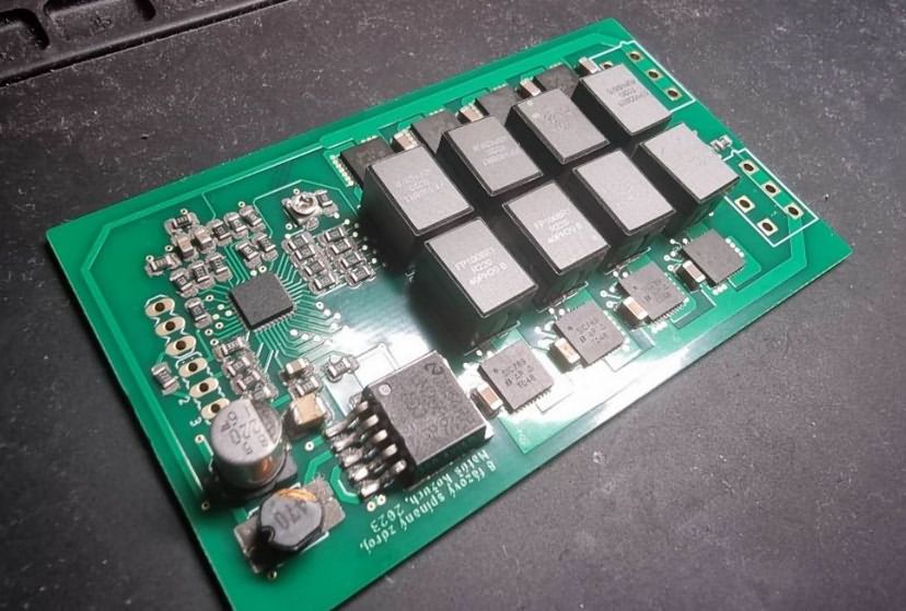
The designed external DC-DC regulator is equipped with an eight-phase integrated controller that detects and balances the output voltage and current of each phase, as well as providing overcurrent and short circuit protection.
Block diagram of a new generation graphics card.
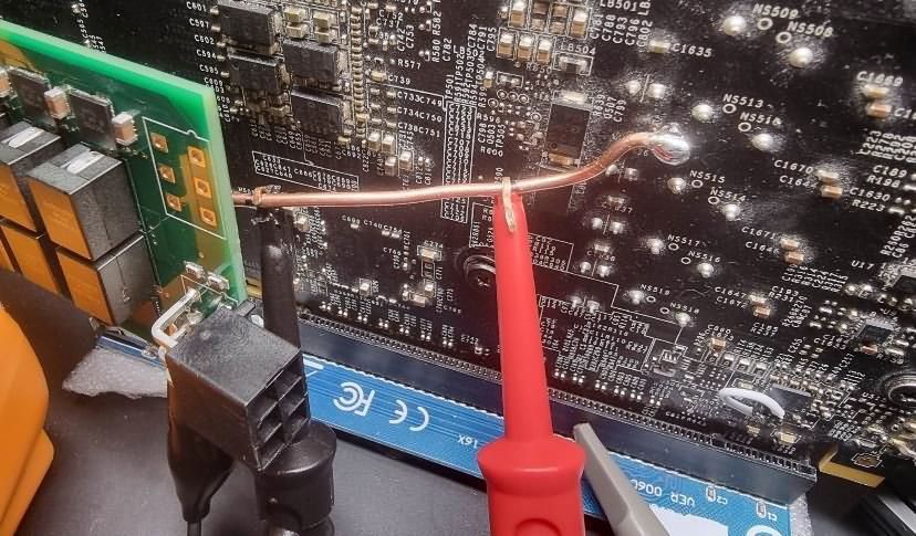
The control and measurement electronics of the circuit are sensitive to voltage induced in the measurement paths and to interference from the controller’s feedback loop, so it is necessary to shield the control part of the circuit well and physically separate it from the power part. The shielding is provided by the copper surface on the two PCB layers below the entire control circuit, which is connected to ground.
However, in addition to shielding, these surfaces are also used to power the individual circuits; therefore, they are connected in such a way that a low-induction connection is made between the individual components for proper communication and minimum noise.
In addition to shielding, it is also necessary to isolate the circuit from the ground noise of the power electronics. This is achieved by connecting the grounds of these circuits with a thin path, the inductance of which prevents the high-frequency switching noise of the power part and spikes from penetrating the control circuit.
Power electronics
The operation of the switching elements of the power electronics with tens of amperes at full load power causes large voltage drops and significant losses in the thin PCB paths, causing them to heat up, so their resistance must be minimized.
This is achieved by maximizing the shortest possible length and width of the paths that direct the switching currents between the individual components from the power supply to the load.
Since the power section consists of up to eight switching elements, their correct distribution is essential for minimum losses. We proposed the best solution to split the switching elements in two and connect them back to back. For good noise characteristics, the order of the individual phases of the switching elements was chosen so that the elements are opposite each other in opposite phases; this results in a uniform loading of the conductive paths and does not increase the noise of the switches.
This distribution of the components creates a short and wide conductive path in the middle of the PCB, to which the load can be directly connected and where there is a minimum voltage drop. It is also possible to achieve precise regulation by connecting the voltage feedback of the control electronics.
Ltspice Circuit Diagram
![]()