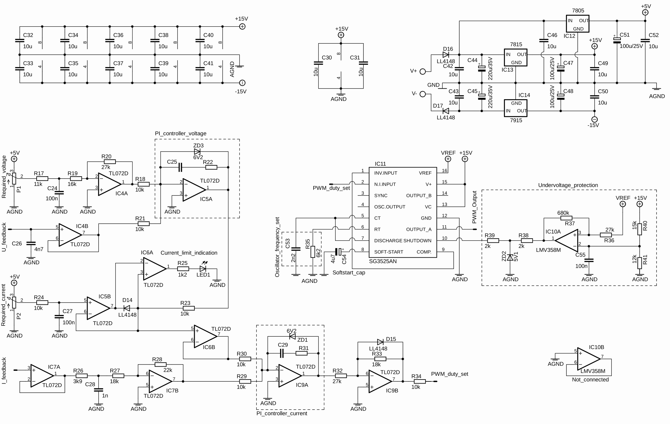
SG3525 Adjustable SMPS 0-30V 0-5A Laboratory Switching Power Supply The SG3525A circuit was selected as the PWM modulator for controlling the switching power supply. It is a PWM modulator specially designed for control of switching power supplies. It has it two complementary outputs of the PWM signal, alternating one output can only range from 0 to 0.49. For this reason, this one the modulator type is suitable for controlling both double-acting (both outputs are used) and single-acting (only one output is used) of the inverters.
The output signal from the control structure is fed to the non-inverting input 2 (NIV.INPUT) internal error amplifier. Inverting input 1 (Noninv.INPUT) is connected to output 9 (Compensation) and the whole connection of the error amplifier thus behaves as voltage tracker. Input voltage level of control signal applied to non-inverting according to the technical documentation [12], input 2 can range from 0.9𝑉 up to 3.6𝑉, while the voltage value of 0.9𝑉 corresponds to zero duty cycle of the output PWM signal and a value of 3.6𝑉 of its maximum (ie a shift of 0.49). Output 3 (SYNC) is specified for external control by clock signal and together with output 4 (OSC.OUTPUT)
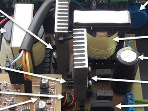
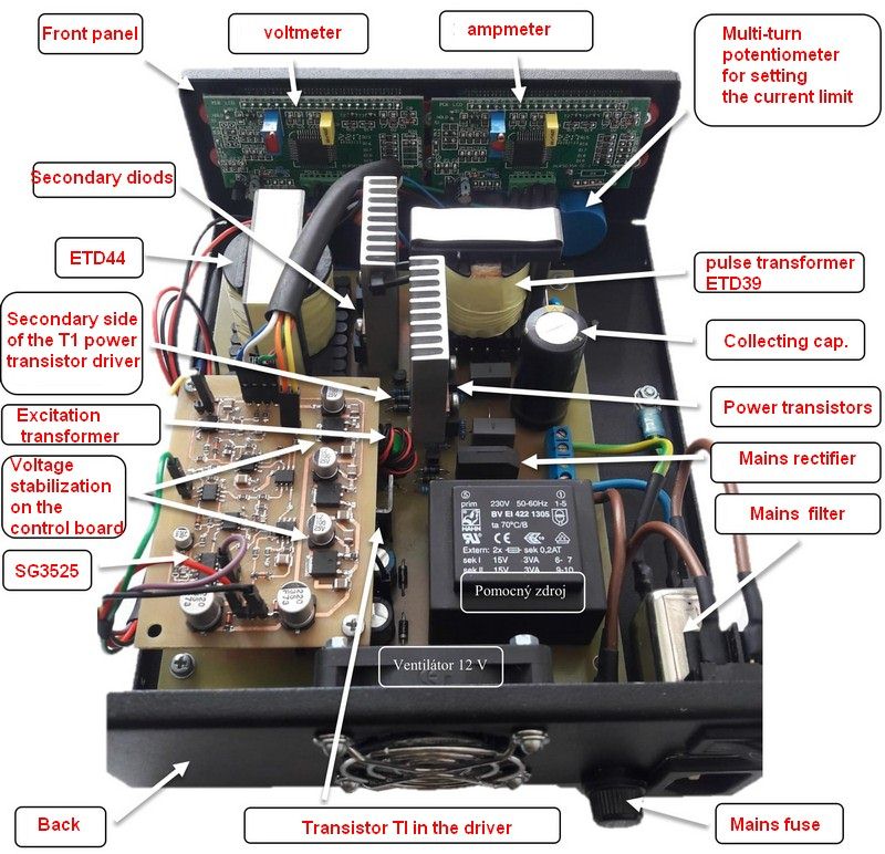
Regulatory structure The control structure of the proposed switching power supply will be implemented as a cascade output voltage regulation with slave current loop The current loop begins by sensing a current signal on a shunt that has a resistance 0, 02Ω (implemented by five SMD resistors in parallel in packages 1206, each with resistance 0, 1Ω). At a maximum current load of 5𝐴, it occurs on this shunt voltage drop 0, 1𝑉, which is sensed by integrated circuit INA213. This is Current monitor specially designed to amplify the current signal from the shunt (during implementation, it is necessary to place this circuit next to the current shunt and prevent thus causing interference).
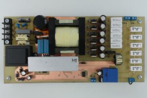
SG3525 0-30 V 0-5 A SMPS Power Supply Circuit Schematic
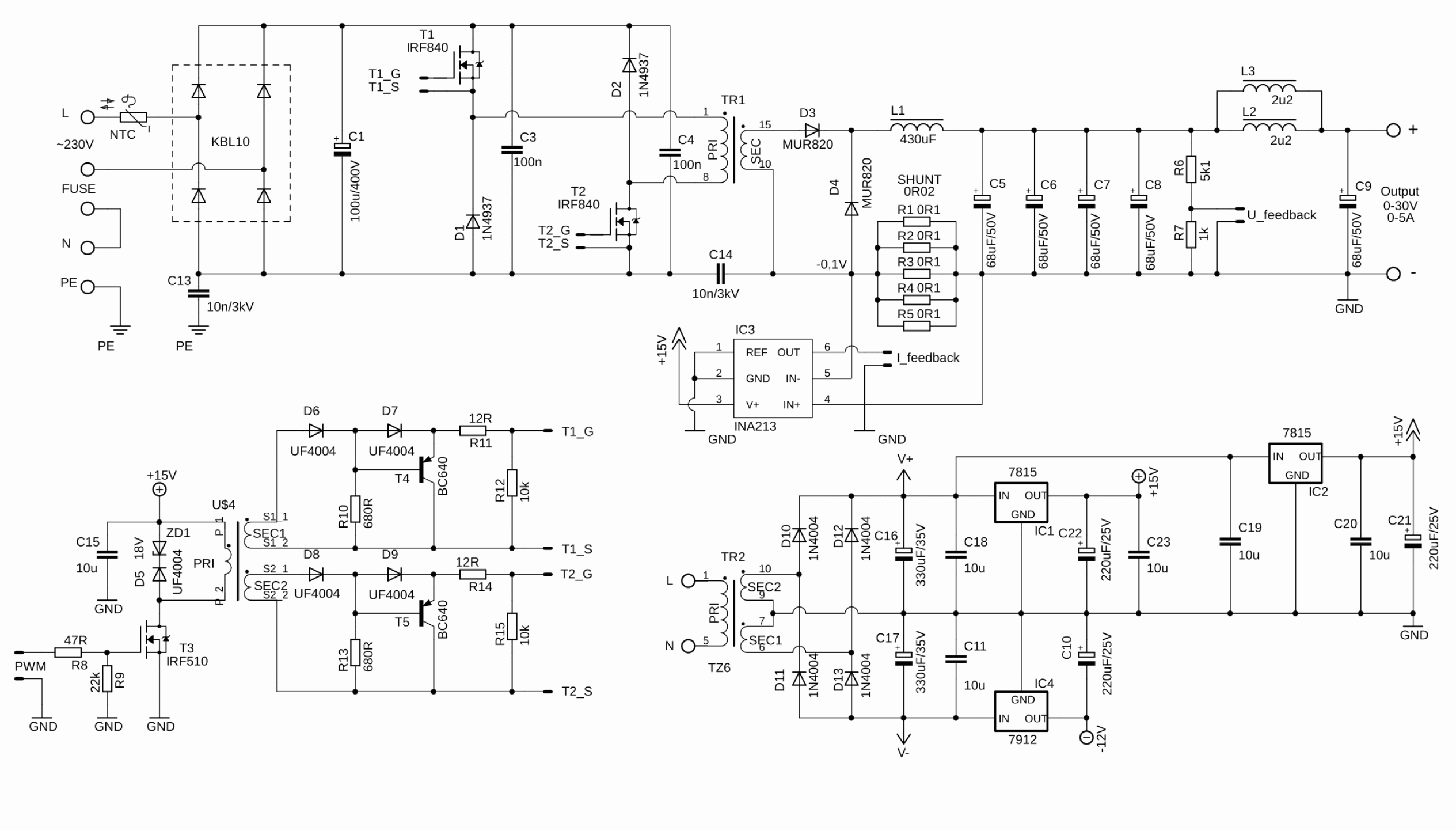
The INA213 circuit is connected to the shunt by two terminals, where the 𝐼𝑁 + terminal is connected to a higher potential (GND) and terminal 𝐼𝑁− to a lower potential The differential voltage between these terminals is then internal amplified by the circuit (50 times for this particular type) and output (OUT). The voltage at this terminal is related to the reference pin (REF), which, how is evident from Fig.2.12, is connected to the common ground GND resp. AGND. The resulting the voltage then appears at the output (OUT) at full load as 0.1𝑉 against ground GND resp. AGND.
![]()
FILE DOWNLOAD LINK LIST (in TXT format): LINKS-26519b.zip

Alimentation de commutation de laboratoire de SG3525 SMPS 0-30 V 0-5 A
SG3525 SMPS réglable 0-30V 0-5A Alimentation à découpage de laboratoire Le circuit SG3525A a été sélectionné comme modulateur PWM pour contrôler l’alimentation à découpage. Il s’agit d’un modulateur PWM spécialement conçu pour le contrôle des alimentations à découpage. Il possède deux sorties complémentaires du signal PWM, une seule sortie alternée ne pouvant aller que de 0 à 0,49. Pour cette raison, celui-ci, le type de modulateur, convient pour contrôler à la fois les onduleurs à double effet (les deux sorties sont utilisées) et à simple effet (une seule sortie est utilisée).
Le signal de sortie de la structure de commande est envoyé à l’amplificateur d’erreur interne d’entrée non inverseuse 2 (NIV.INPUT). L’entrée inverseuse 1 (Noninv.INPUT) est connectée à la sortie 9 (Compensation) et toute la connexion de l’amplificateur d’erreur se comporte donc comme un tracker de tension. Niveau de tension d’entrée du signal de commande appliqué au non inverseur selon la documentation technique [12], l’entrée 2 peut aller de 0,9𝑉 à 3,6𝑉, tandis que la valeur de tension de 0,9𝑉 correspond à un rapport cyclique nul du signal PWM de sortie et une valeur de 3,6𝑉 de son maximum (soit un décalage de 0,49). La sortie 3 (SYNC) est spécifiée pour le contrôle externe par signal d’horloge et avec la sortie 4 (OSC.OUTPUT)
Structure de régulation La structure de contrôle de l’alimentation à découpage proposée sera implémentée comme une régulation de tension de sortie en cascade avec boucle de courant esclave La boucle de courant commence par détecter un signal de courant sur un shunt qui a une résistance 0, 02Ω (implémentée par cinq résistances SMD dans parallèle en boîtiers 1206, chacun avec résistance 0, 1Ω). À une charge de courant maximale de 5𝐴, il se produit sur cette chute de tension de shunt 0, 1𝑉, qui est détectée par le circuit intégré INA213. Il s’agit d’un moniteur de courant spécialement conçu pour amplifier le signal de courant du shunt (lors de la mise en œuvre, il est nécessaire de placer ce circuit à côté du shunt de courant et d’éviter ainsi de provoquer des interférences).