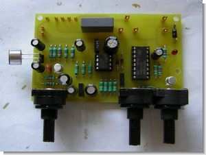
The circuit turns the relay on and off according to the sound intensity in the environment, and its sensitivity can be adjusted with rv1 rv2 100k potentiometers. In the amplifier section, LM358 opamp is used and in the driver stage, the on time of the CD4528 relay can be adjusted by changing the RV3 setting and C11, R18 resistor and capacitor values. The circuit has proteus isis circuit diagram and ares pcb drawings.
The sound detector mentioned here is designed to operate a recording device or turn on a filament light bulb as soon as a sound picked up by a small microphone exceeds a predetermined volume level.
The sensitivity range is very wide, the mount can respond to a spoken sound five meters away from the microphone. Of course, this kind of precision is not always desired and the assembly has a setting that allows you to tailor it to your own needs. I made this installation after a holiday center manager wanted to have a “noise overflow warning lamp” installed in the cafeteria. A history of setting boundaries that should not be crossed with the children at mealtimes. It’s not easy, knowing that the game can also consist of making as much noise as possible to light the lamp… Isn’t it all about setting the rules exactly?
Of course, there are much simpler circuits than this, and they are content with a single transistor or a single integrated circuit as the active element. To put it right away, I developed this diagram with the desire to have something that is perfectly reproducible and works well every time. I didn’t try to make it simpler, because in this case wanting to make it simpler would be synonymous with difficulty. In this diagram, no component is truly critical and it’s okay to get an approximation for each. The assembly consists of five different parts, which I will describe separately: a microphone preamplifier, a diode rectifier, a comparator, a monostable (timer) and a power output stage.
Sound Detector Project

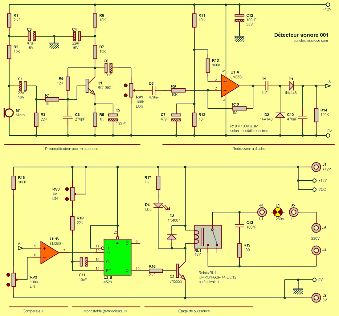
Microphone preamplifier
The microphone preamp is based on the use of a current transistor. But why didn’t you use the diagram that appears on the Preamp page for the single mic 001? It should be simpler and sufficient, right? This is a good question. Also, if you look closely, there isn’t much difference between the 001 preamp schematic and the schematic on this page. The main differences lie in the addition of a resistor R6 to the emitter circuit of the BC109 (Q1) to ensure good thermal stabilization, which guarantees stable operation even with strong changes in ambient temperature.
Since this resistance is quite high (given its location) and strongly reduces the gain of the amplification stage, a 100uF capacitor C2 is added in parallel with it. Second, in static mode it behaves like an open circuit and does not affect the DC bias of the transistor, and in dynamic mode it almost behaves like a short circuit when a BF signal is present at the input. So this capacitor makes it possible to “recover” the gain lost due to the emitter resistor.
The 12 K resistor R5 plays on the fundamental polarization of Q1, where it also plays on the gain, which is close to 20 dB. If you find this gain insufficient, you can increase the value of R5 to 220 K, for which the gain is about 32 dB or It will be 12 dB more. The microphone used is of the electret capsule type, chosen for its compactness, high sensitivity and very low cost. If you prefer to use a small 200 ohm dynamic microphone you can, but in that case do not wire the R1, R2 and C3 components used here for the microphone. It needs power to work). The RC cell consisting of R1 and C3 is absolutely necessary, it makes it possible to isolate the microphone’s power supply from the rest of the assembly. Without this decoupling cell, there would be a high risk of this preamp stage starting to oscillate.
Note that the supply of transistor Q1 also goes through quite strong decoupling for the same reasons. The amplified signal exits the collector of transistor Q1 and passes through a coupling capacitor intended to prevent the DC voltage present in the collector from reaching the subsequent sensitivity adjustment potentiometer.
The diode rectifier in question here is based on the use of an LM358 type AOP integrated circuit that amplifies the BF signal a little before rectifying it, ie converting the signal to a DC voltage proportional to the amplitude of the signal it receives. Microphone. This section is not based on the famous architecture where the rectifier diode is placed in the feedback loop of the AOP to suppress the diode’s conduction threshold. There is no need for this trick, which we will gladly leave to more detailed assemblies here. The signal to be processed is taken from the slider of the potentiometer.
Used here as a sensitivity setting and applied to the inverting input of AOP U1:A, the first half of the LM358. The amplification rate of this second stage is high, its value here determined by the ratio between the two resistors R10 and R9, which is 100 (corresponding to 40 dB). If the sensitivity of the assembly seems too high to you in a practical situation, feel free to lower the R10 value to 100K or even less. When the LF signal is amplified again, it is applied to the rectifier part consisting of C9, C10, D1, D2 and R14. On the cathode of D1 (common of D1, C10 and R14) there is a DC voltage proportional to the amplitude of the BF signal applied to the rectifier input (common point R10 / C9). The only thing left
Comparator This is the simplest part of the assembly, using only three components U1:B (second half of LM358), R15 and RV2. Output 7 of AOP U1:B is high (12V), when the voltage available at input 5 (+) is higher than the voltage available at input 6 (-) (12V). However, when the voltage at input 5 (+) is lower than the voltage at input 6 (-), the same output is in a low state (0V). Since the rectified voltage applied to input 5 (+) is even higher than the received sound is strong, there is a moment when this voltage will exceed the reference voltage (at terminal 6), causing the output to switch the AOP. from low to high. So you understand that there is a second setting that will determine the trigger threshold, and that you will need to find a good compromise between the two settings offered by the RV1 and RV2. Note, however, that for simplicity you can completely replace the RV2 potentiometer with a fixed resistor from 1K to 4K7, thus keeping only the RV1 setting. Personally, I prefer to keep this RV2 potentiometer, which simplifies settings in extreme sensitivity situations.
Timer This section has been added to guarantee a minimum trigger time regardless of the time the audio signal received by the microphone exceeds the switching threshold. The circuit is based on the use of monostable type CD4528 or CD4538, which produces a pulse of perfectly defined width when applied to the trigger input.
“positive”, a rising edge (logic level that goes from low to high), this is the previous a when the captured sound is strong enoughis the exact state of the shaman. The activation time (pulse width) of the output is determined by the value of components C11, R18 and RV3 and can be adjusted from just under 1 second to about ten seconds. Note that the second half of CD4528 (4538) is used, and this is only to facilitate routing of the IC. The first half would also be quite appropriate! As it is not in use, the trigger and reset inputs are connected to ground to stay at a perfectly fixed potential and thus prevent “flickering” from one state to the next.
Power output stage
This stage is necessary to be able to control loads other than a small low voltage lamp or an LED. The use of a relay here is justified by the fact that the controlled circuit could be inductive (tape on K7 with a transformer for the power supply), and this would be a problem if the output were made with a triac. The relay is controlled by a universal type NPN transistor, type 2N2222. This transistor is protected by diode D3 against overvoltages caused by the relay when disabled. The relay should be selected according to the power consumed by the device to be controlled, its contacts should be able to withstand the switched current. led _D4 serves as a local witness and is optional. A series RC cell (C13 / R19) has been added in parallel with the contacts to ensure longer life of the relay contacts, this prevents sparking during switching.
source: sonelec-musique.com Sound Detector schematic Circuit files alternative link:

150W Power Amplifier Circuit MJ21194 MJ21193 Transistor
Quality power Amplifier circuit a famous brand’s clone version of the “Krell KSA-50” 8Ω speaker with a 70w rms power can give is said output transistors mj21193 and mj21194 circuit schematic, printed circuit board views from the top all the drawings and gerber files are
Krell Clone 150W Amplifier Circuit