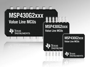
Texas Instruments MSP430 MCU series microcontrollers `s prepared for hundreds of applications with C language prepared sample codes (IAR Embedded Workbench Version 3.41 A) in the comment section of code specified in their use.
MSP430F543x MSP430F541x MSP430 examples
msp430x54x_adc12_01.c ADC12, Sample A0, Set P1.0 if A0 > 0.5*AVcc
msp430x54x_adc12_02.c ADC12, Using the Internal Reference
msp430x54x_adc12_05.c ADC12, Using an External Reference
msp430x54x_adc12_06.c ADC12, Repeated Sequence of Conversions
msp430x54x_adc12_07.c ADC12, Repeated Single Channel Conversions
msp430x54x_adc12_08.c ADC12, Using A8 and A9 Ext Channels for Conversion
msp430x54x_adc12_09.c ADC12, Sequence of Conversions (non-repeated)
msp430x54x_adc12_10.c ADC12, Sample A10 Temp and Convert to oC and oF
msp430x54x_dma_01.c DMA0, Repeated Block to-from RAM, Software Trigger
msp430x54x_dma_02.c DMA0, Single Transfer in Block Mode UART1 9600, ACLK
msp430x54x_dma_03.c SPI TX & RX using DMA0 & DMA1 Single Transfer in Fixed Address Mode
msp430x54x_dma_04.c DMA0, Single transfer using ADC12 triggered by TimerB
msp430x54x_fet_1.c Software Toggle P1.0
msp430x54x_flashwrite_01.c Single-Byte Flash In-System Programming, Copy SegC to SegD
msp430x54x_flashwrite_02.c Flash In-System Programming w/ Long-Word write at 0x1800
msp430x54x_flashwrite_03.c Bank Erase from a Block while Executing Code from Another Block.
msp430x54x_flashwrite_04.zip Block Write and Memory Erase @ 0x10000 Executed from RAM
RTC_Workaround.zip RTC_Workaround_IAR, RTC_Workaround_CCE
msp430x54x_LPM3_1.c Enters LPM3 (ACLK = LFXT1)
msp430x54x_LPM3_2.c Enters LPM3 (ACLK = VLO)
msp430x54x_MPY_1.c 16×16 Unsigned Multiply
msp430x54x_MPY_2.c 8×8 Unsigned Multiply
msp430x54x_MPY_3.c 16×16 Signed Multiply
msp430x54x_MPY_4.c 8×8 Signed Multiply
msp430x54x_MPY_5.c 16×16 Unsigned Multiply Accumulate
msp430x54x_MPY_6.c 8×8 Unsigned Multiply Accumulate
msp430x54x_MPY_7.c 16×16 Signed Multiply Accumulate
msp430x54x_MPY_8.c 8×8 Signed Multiply Accumulate
msp430x54x_MPY_9.c 32×32 Unsigned Multiply
msp430x54x_MPY_10.c 32×32 Signed Multiply
msp430x54x_MPY_11.c 32×32 Signed Multiply Accumalate
msp430x54x_MPY_12.c 32×32 Unsigned Multiply Accumalate
msp430x54x_MPY_13.c Saturation mode overflow test
msp430x54x_MPY_14.c Saturation mode underflow test
msp430x54x_MPY_15.c Fractional mode, Q15 multiplication
msp430x54x_OF_LFXT1_nmi.c LFXT1 Oscillator Fault Detection
msp430x54x_P1_01.c Software Poll P1.4, Set P1.0 if P1.4 = 1
msp430x54x_P1_02.c Software Port Interrupt Service on P1.4 from LPM4 with Internal Pull-up Resistance Enabled
msp430x54x_P1_05.c Write a byte to Port 1
msp430x54x_PA_05.c Write a Word to Port A (Port1+Port2)
msp430x54x_RTC_01.c RTC in Counter Mode toggles P1.0 every 1s
msp430x54x_ta3_01.c Timer_A3, Toggle P1.0, CCR0 Cont. Mode ISR, DCO SMCLK
msp430x54x_ta3_02.c Timer_A3, Toggle P1.0, CCR0 Up Mode ISR, DCO SMCLK
msp430x54x_ta3_03.c Timer_A3, Toggle P1.0, Overflow ISR, DCO SMCLK
msp430x54x_ta3_04.c Timer_A3, Toggle P1.0, Overflow ISR, 32kHz ACLK
msp430x54x_ta3_05.c Timer_A3, Toggle P1.0, CCR0 Up Mode ISR, 32kHz ACLK
msp430x54x_ta3_08.c Timer_A3, Toggle P1.0;P2.1-3, Cont. Mode ISR, 32kHz ACLK
msp430x54x_ta3_11.c Timer_A3, Toggle P2.1/TA1.0, Up Mode, 32kHz ACLK
msp430x54x_ta3_13.c Timer_A3, Toggle P2.1/TA1.0, Up/Down Mode, DCO SMCLK
msp430x54x_ta3_14.c Timer_A3, Toggle P2.1/TA1.0, Up/Down Mode, 32kHz ACLK
msp430x54x_ta3_16.c Timer_A3, PWM TA1.1-2, Up Mode, DCO SMCLK
msp430x54x_ta3_17.c Timer_A3, PWM TA1.1-2, Up Mode, 32kHz ACLK
msp430x54x_ta3_19.c Timer_A3, PWM TA1.1-2, Up/Down Mode, DCO SMCLK
msp430x54x_ta3_20.c Timer_A3, PWM TA1.1-2, Up/Down Mode, 32kHz ACLK
msp430x54x_tb_01.c Timer_B, Toggle P1.0, CCR0 Cont. Mode ISR, DCO SMCLK
msp430x54x_tb_02.c Timer_B, Toggle P1.0, CCR0 Up Mode ISR, DCO SMCLK
msp430x54x_tb_03.c Timer_B, Toggle P1.0, Overflow ISR, DCO SMCLK
msp430x54x_tb_04.c Timer_B, Toggle P1.0, Overflow ISR, 32kHz ACLK
msp430x54x_tb_05.c Timer_B, Toggle P1.0, CCR0 Up Mode ISR, 32kHz ACLK
msp430x54x_tb_10.c Timer_B, PWM TB1-6, Up Mode, DCO SMCLK
msp430x54x_UCS_1.c Software Toggle P1.0 at Default DCO
msp430x54x_UCS_2.c Software Toggle P1.0 with 8MHz DCO
msp430x54x_UCS_3.c Software Toggle P1.0 with 12MHz DCO
msp430x54x_UCS_4.c FLL+, Runs Internal DCO at 2.45MHz with LFXT1 as Ref
msp430x54x_UCS_5.c VLO sources ACLK
msp430x54x_UCS_6.c XT1 sources ACLK. Toggles P1.0
msp430x54x_UCS_7.c FLL+, Output 32kHz Xtal + HF Xtal + Internal DCO
msp430x54x_UCS_8.c XT2 sources MCLK & SMCLK
msp430x54x_UCS_9.c LFXT1 HF Xtal + Internal DCO
msp430x54x_uscia0_duplex_9600.c USCI_A0, UART 9600 Full-Duplex Transceiver, 32K ACLK
MSP430x54x_uscia0_spi_09.c USCI_A0, SPI 3-Wire Master Incremented Data
MSP430x54x_uscia0_spi_10.c USCI_A0, SPI 3-Wire Slave Data Echo
MSP430x54x_uscia0_uart_01.c USCI_A0, 115200 UART Echo ISR, DCO SMCLK
MSP430x54x_uscia0_uart_02.c USCI_A0, Ultra-Low Pwr UART 2400 Echo ISR, 32kHz ACLK
MSP430x54x_uscia0_uart_03.c USCI_A0, Ultra-Low Pwr UART 9600 Echo ISR, 32kHz ACLK
MSP430x54x_uscia0_uart_04.c USCI_A0, 9600 UART, SMCLK, LPM0, Echo with over-sampling
MSP430x54x_uscib0_i2c_04.c USCI_B0 I2C Master RX single bytes from MSP430 Master
MSP430x54x_uscib0_i2c_05.c USCI_B0 I2C Slave TX single bytes to MSP430 Slave
MSP430x54x_uscib0_i2c_06.c USCI_B0 I2C Master TX single bytes to MSP430 Slave
MSP430x54x_uscib0_i2c_07.c USCI_B0 I2C Slave RX single bytes from MSP430 Master
MSP430x54x_uscib0_i2c_08.c USCI_B0 I2C Master TX multiple bytes to MSP430 Slave
MSP430x54x_uscib0_i2c_09.c USCI_B0 I2C Slave RX multiple bytes from MSP430 Master
MSP430x54x_uscib0_i2c_10.c USCI_B0 I2C Master RX multiple bytes from MSP430 Slave
MSP430x54x_uscib0_i2c_11.c USCI_B0 I2C Slave TX multiple bytes to MSP430 Master
MSP430x54x_wdt_01.c WDT, Toggle P1.0, Interval Overflow ISR, DCO SMCLK
MSP430x54x_wdt_02.c WDT, Toggle P1.0, Interval Overflow ISR, 32kHz ACLK
MSP430x54x_wdt_04.c WDT+ Failsafe Clock, WDT mode, DCO SMCLK
MSP430x54x_wdt_05.c Reset on Invalid Address fetch, Toggle P1.0
Published: 2010/10/17 Tags: microcontroller projects, msp430 projects, pwm circuits
Digital PLL controlled FM Radio Circuit TEA5767 Receiver PIC16F628
Yes, let’s recent project, a “Digital and PLL controlled FM Radio Receiver System” will give. Some of them may sound like a simple project. But a very open system development project. Currently on the market that has all the features of most modern radio despite the limited resources, why did the simplistic with this project. This is a fully digital PLL controlled FM radio project.
Digital PLL controlled FM Radio Proteus isis circuit