The reproducibility of DC-CDI in most implementers faces the difficulty and little experience of transformer winding. Therefore, this design, based on DC-CDI is used to transform the voltage using a PC power transformer EI-33. So there is no need to wind up any transformer.
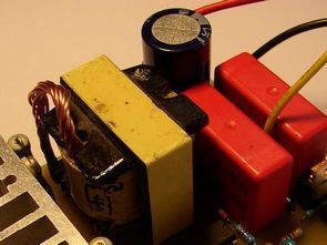
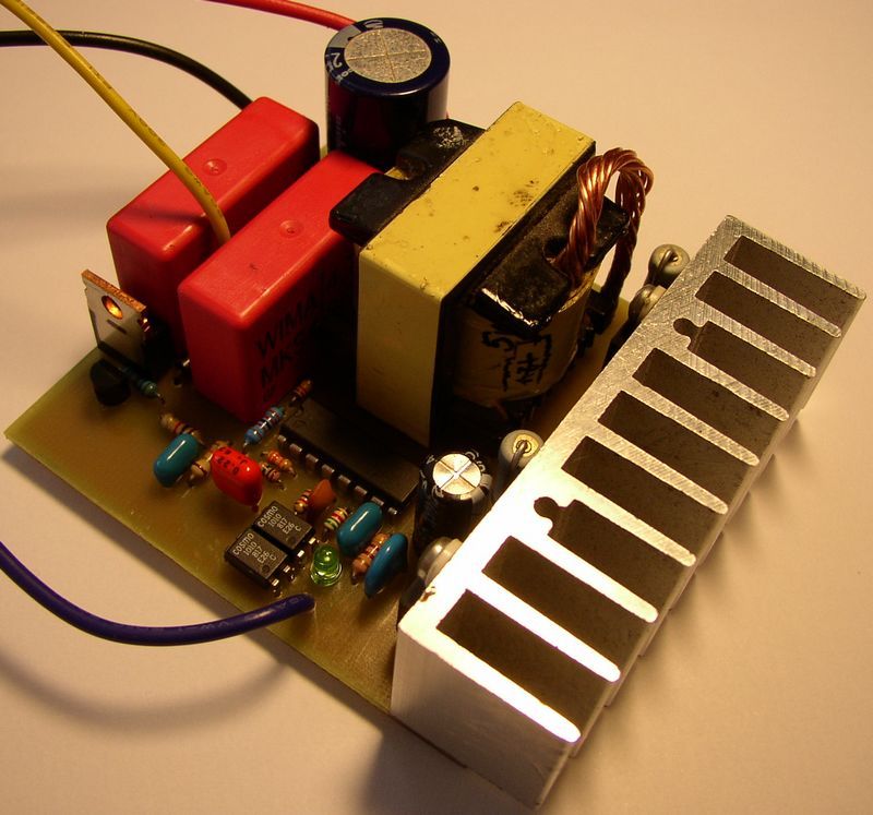
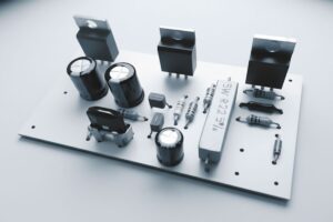
The necessary EI-33 transformer can be obtained from older types of PCs. The easiest to know is that the source contains (most often) a common, independently guided GND transformer output (braided wires see photo). And most often as a control integrated circuit is used TL494 or some of its Asian clone (KA7500, KIA494 etc.)
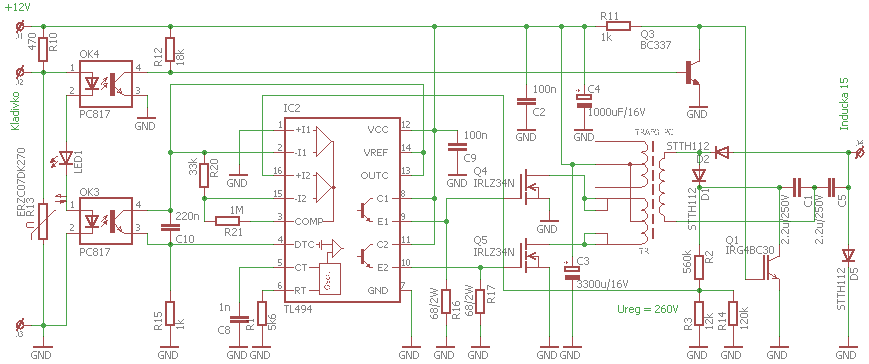
The EI-33 transformer usually contains two symmetrical secondary windings for 12V and 5V distributions with a common center of both windings. Thus, the direction of transformation can be rotated in a simple way. Transformers are always wound up for 120V (and 230V) wiring, so we only get 150V when rotating the transformer, which is very little for proper CDI operation. Thus, the output portion contains a voltage doubler D1, D2, C1 and C5, as opposed to the conventional CDI version. Discharging capacities (spark ignition spark plug) is provided by IGBT transistor Q1. The input section contains a pair of insulating optocouplers that provide galvanic isolation of the input of the inverter from the excitation part of the ignition (eg hammer, hall, optocoupler) and with the control LED1 it forms one unit in series. LED1 is wired to optically check the optron functionality.
The EI33 PC transformer is very powerful and, after ignition and full discharge of its capacities, it loads the power supply cables and smoothing capacitors with its power and appears to be a short circuit for a very short time. This secondary caused a great supply voltage interference and poor condenser voltage build-up and unnecessary overheating of the transistors. Increasing capacities and smoothing out voltage by blocking capacities would only result in a poor result and therefore the circuit also includes a simple RC cell (R15 and C10) to provide a soft start-up voltage from the transformer. By changing the values, the slope can be further suppressed. The resistor divider R2 / R3 + R14 forms a cell that controls the stabilized maximum output voltage of the inverter. The connection is tuned to 260V. For the simplicity of the TL494 power outputs, the resistors R16 and R17 are connected to ensure the discharge of the GATE MOSFET capacitors and thus ensure a sufficiently fast closing of the transistors Q4 and Q5. The R1 resistor tunes the optimum frequency for the transformer
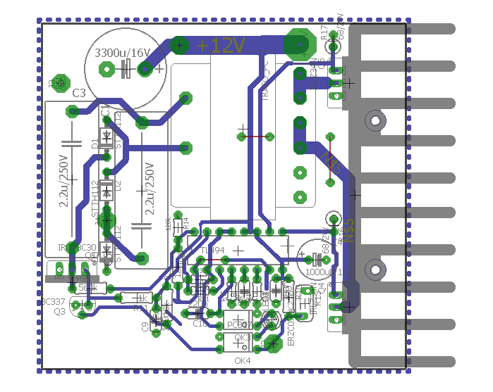
Place the board (including heat sinks) outside the resistors R1, R2 and Q1 transistor. Resistor R1 is temporarily replaced by trimmer 100k. The “hammer” input wire and “induck 15” output wire will ground to GND.
A power resistance (at least 10W) of 4k7 is applied between the inverter positive voltage output (cathode D1) and GND. A voltmeter over 300V is connected between the power resistor terminals and a current meter is connected to the power supply wires.
CDI Circuit schematic
After connecting the power supply (a sufficiently strong stabilized 12V source, or a charged 12V battery), the trimmer tunes the highest voltage on the power resistance terminals (should be around 300V) at the lowest possible current consumption. After finding the optimum resistance value, the power-up readiness must be tested by repeatedly disconnecting and connecting the power while monitoring the output voltage and input current stability. If the inverter readily responds to this frequency, remove the trimmer and replace its resistance with the closest fixed resistance value, again testing the reliability of the inverter voltage rise. It is advisable to test the properties even at low voltages of around 10V, as well as at voltages close to that of the battery, ie 14.4V.
Subsequently, the resistor R2 is fitted, whereby the output voltage should be stabilized at about 260V when the converter is switched on. The change of the output voltage can be changed by changing the values of resistors R2, R3 and R14 (R14 serves only for fine tuning of the output voltage).
Now it is possible to remove the power resistor and install the transistor Q1. After connecting the power supply, the consumption should be negligible, thus testing that Q1 is not damaged and does not block the drive output with a short circuit.
This brings the revival to an end. Care must be taken to ensure that the CDI input is not connected to + power supply in any case, the outlet may only be connected to ground, otherwise the input optocouplers and LEDs will be destroyed! It is not recommended to use the output without connecting it to an inductor.
You can find the documentation for CDI production HERE.
The CDI can be used for single cylinder and two cylinder engines. When used for ignition of a two-cylinder engine, a two-lead ignition coil is connected to the CDI output, which is coupled to both candles. The ignition cut is then designed to ignite at both dead and top dead center on both cylinders.
Source : btelectronic.sweb.cz
FILE DOWNLOAD LINK LIST (in TXT format): LINKS-26190.zip

600W LED Dimmer Circuit PFC ICE2PCS01 UCC28C43
600W LED Dimmer Circuit PFC ICE2PCS01 UCC28C43
This block is used to reduce and stabilize the voltage produced by the PFC block. The output voltage of this block is controlled by the control signal. Since the output voltage is higher than the safe touch (according to the CSN standard), it is possible to use the lower switch at the lowering drive. UCC28C43 integrated circuit is used for control
First, a part of the PFC was fitted to make it easier to locate any faults. The peripheral components of this block have been installed and run through a series-connected bulb that serves as a protection against a possible short circuit. The figure (Fig. 3.3) contains the oscillogram with the control voltage and voltage on the transistor Q1 without loading the PFC output. The load on the PFC load was gradually connected to the output of which the power loss 140, 330, 500 and 660 W was generated. contain oscilloscope with PFC voltage waveforms at 660 W and input Voltage 220 V. The waveform of the input current is approximately sinusoidal. The mean voltage of the PFC output is 370 V. The voltage ripple is 16 volts.
This chapter describes the design of the dimmer as a whole. Requirements for it are:
adjustable DC output voltage up to Uout_BUCK = 285 V,
output power Pout_BUCK = 600 W (at output voltage Uout_BUCK)
AC input voltage in the range Uin_min_PFC = 190 to Uin_max_PFC = 260 V
Output voltage control via external PWM signal
power components on a common heat sink,
high dimmer power factor.
CDI Circuit TL494 PC transformateur de puissance EI33
La reproductibilité du DC-CDI dans la plupart des implémenteurs est confrontée à la difficulté et au peu d’expérience de l’enroulement du transformateur. Par conséquent, cette conception, basée sur DC-CDI, est utilisée pour transformer la tension à l’aide d’un transformateur de puissance PC EI-33. Il n’est donc pas nécessaire d’enrouler un transformateur.
Le transformateur EI-33 nécessaire peut être obtenu à partir d’anciens types de PC. Le plus simple à savoir est que la source contient (le plus souvent) une sortie de transformateur GND guidée indépendamment (fils tressés voir photo). Et le plus souvent, un circuit intégré de contrôle est utilisé TL494 ou une partie de son clone asiatique (KA7500, KIA494, etc.)