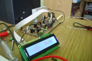
PT2240, PT2262, HT6P20B RF Transceiver ICs were cloned as software and application circuits were made with microcontroller. Clone circuits may be higher in cost, but it is a very good resource in terms of software. It is very difficult to put the working system of ICs such as PT2240, PT2262 into software. HT6P20B PT2240 PT2262 Clone applications have source software files and application schematics.
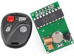
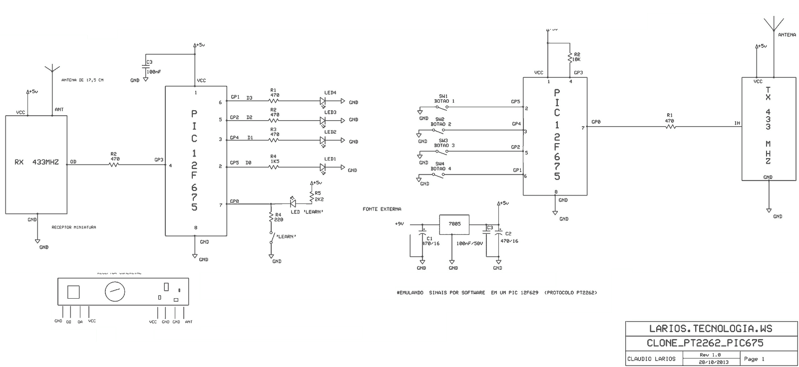
PT2262 Clone Circuit
You can use PIC12F675 or PIC12F629. The PT2262 protocol is interesting because it is ‘triple’, that is, it allows 3 different configurations on the addressing pins (equivalent to a serial number). Thus, we can connect these pins to VCC or GND via jumpers or leave them blank. This allows up to 531441 different addresses (serial number) to be received.
In the ASM file, we can define which configuration we want for the pins in the equations. It will be equivalent to connecting to null or VCC or even GND. In the PT2262 there is a resistor responsible for the frequency of the internal oscillator, which defines the times of the bits.
Its value can be between 470K and 4M7 and it generates frequency from 5 to 50 KHZ. In this setup, a delay value was chosen that roughly corresponds to the 4M7 resistor. For other values, you will need to change the value of the ‘T_PULSO’ equation.
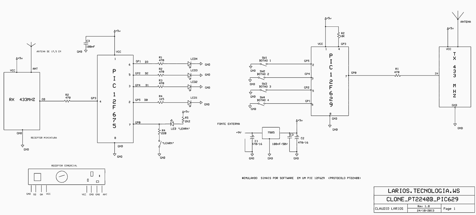
PT2240 Clone Circuit
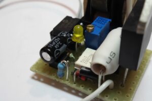
A PIC12F675 was used to software-generate the protocol used in the PT2240 (with a minor change to asm, you can use the PIC12F629). Only a few simple components are required, such as switches, resistors, capacitors, plus a 433 mhz rf transceiver.
Talking a bit about the PT2240 protocol, it sends a total of 20 address bits plus 4 data bits in series, and there is a sync bit at the end of the transmission to synchronize the transmission. How to distinguish bit ‘1’ from ‘0’ By transmission time and non-transmitting interval. Thus, bit ‘1’ is achieved by keeping the output in a range that is ‘logical 1’ (sender) for 96 clock cycles and then ‘logical 0’ (not transmit) for 32 clock cycles. Bit ‘0’ is inverted: ‘logical 1’ output for 32 clock cycles and an interval output ‘logical 0’ for 96 clock cycles.
The PT2240 has a pin that takes a resistor to Vcc to define the frequency of the internal oscillator, i.e. the clock mentioned above. In the datasheet, it shows a frequency response curve relative to its value. A high value between 2M and 4M7 appears to be used in most applications. This leaves the frequency close to 100 khz. In the ASM code, it can be changed to equal ‘T_pulso’ and other values that determine this frequency.
The 4 switches change the data bits (D0, D1, D2 and D3) sent in the transmission. The address (serial number) can be changed by changing the values of the ‘Ser0, Ser1 and Ser2’ equivalencies. Then you need to recompile with the help of Mplab_Ide.
Source: picsource.com.br
Alternative File download LINK list (in TXT format) 28488a.zip password: 320volt.com