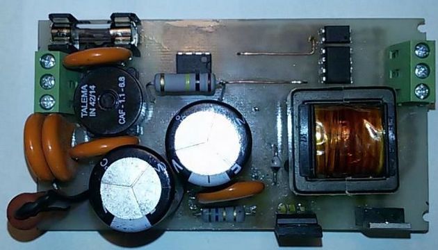
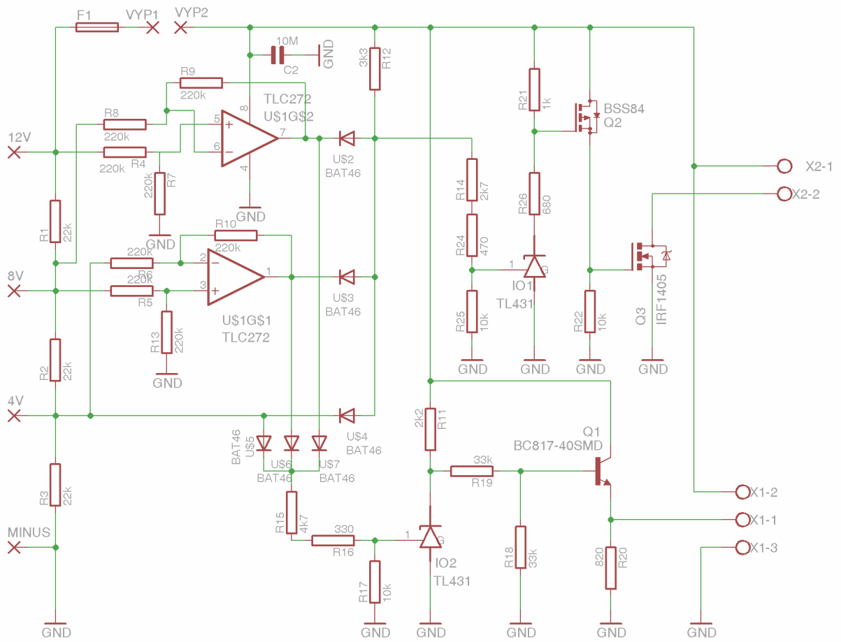
Li-ion 14.4V Battery Pack UC3844 SMPS Charger the UC3844 integrated circuit is supplied directly from the DC link via the resistor R2. After the circuit switches on, the power transistor Q1 is powered by the auxiliary winding. The RCD cell, consisting of R3, capacitor C3 and diode D1, protects the power transistor from positive overflows caused by parasitic inductance.
The transistor Q1 is connected to the output pin 6 of the integrated circuit. On the Zener diode, this output voltage is reduced by 3 V. The capacitor C5 is charged at the same voltage. If the transistor is switched off, this voltage is subtracted from the zero potential and at that moment the negative voltage at the gate of the transistor will be equal to the same value. This ensures a reliable and fast shutdown of the MOSFET.
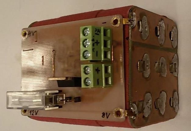
From the BMS battery, an ACCEPTED signal will be transmitted, which corresponds to the log 1 value in case of possible charging, log 0 in the case of charging. This signal is galvanically isolated via the OK2 opto-coupler. In the case of log 1 at the terminal ACCEPTED, log 0 appears at the output of the opto-coupler (pin 6), the signal transistor T2 is closed and the reference voltage from the integrated circuit UC3844 from the pin is displayed on the emitter of the PNP transistor T1 which is connected as a voltage monitor 8. This voltage is applied to pin 1 of the integrated circuit. This state enables the current comparator to switch
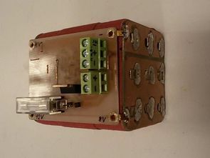
Differential amplifiers U1G1 and U2G2 have the task of converting the differential voltage of the cells connected between the 4V and 8V, 8V and 12V terminals to the ground. Differential amplifiers have gains equal to one, thus unchanged. Via a circuit that consists of U5, U6 and U7 diodes, the voltage at the node is approximately 0.4 volts lower than the highest battery voltage. This voltage is applied to the control input of the integrated parallel stabilizer TL431 (IO2) via the resistive divider. If this voltage is higher than the internal reference voltage of 2.5 V, the output stage transistor opens inside the TL431 and a zero potential appears on the emitter of the PNP transistor Q1, which is connected as a voltage monitor. By changing the zero voltage voltage on the resistive divider formed by the R18 R19, pulses are generated that represent the alternation between charging and charging. These pulses are applied to the STANDED terminal on the switched power source. With increasing battery charge, these pulses will be tightened until the pulse rate is zero at full charge
Li-ion 14.4V Battery Pack Charger schematics
![]()
FILE DOWNLOAD LINK LIST (in TXT format): LINKS-25892.zip
14.4V Li-Ion Batterie Packung UC3844 SMPS Schaltnetzteil Ladegerät
Li-ion 14.4V Batterie Packung UC3844 Schaltnetzteil SMPS Ladegerät Der integrierte Schaltkreis UC3844 wird direkt vom Zwischenkreis über den Widerstand R2 versorgt. Nach dem Einschalten der Schaltung wird der Leistungstransistor Q1 von der Hilfswicklung gespeist.
Die RCD-Zelle, die aus R3, Kondensator C3 und Diode D1 besteht, schützt den Leistungstransistor vor positiven Überläufen, die durch parasitäre Induktivität verursacht werden.
Der Transistor Q1 ist mit dem Ausgangspin 6 der integrierten Schaltung verbunden. Auf der Zenerdiode wird diese Ausgangsspannung um 3 V reduziert. Der Kondensator C5 wird mit der gleichen Spannung geladen. Wenn der Transistor ausgeschaltet ist, wird diese Spannung vom Nullpotential subtrahiert, und zu diesem Zeitpunkt ist die negative Spannung am Gate des Transistors gleich dem gleichen Wert. Dies gewährleistet eine zuverlässige und schnelle Abschaltung des MOSFETs.