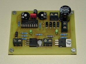
There are motor driver circuits made with TL494 pwm control IC, different circuits powered by low current P channel N channel and N-P channel mosfets without using mosfet. There are schematic drawings prepared with splan and pcb prepared with sprint layout (for n-p two-mosfet circuit).
It is recommended to set up the circuits as shown here. His hobbyist also likes to receive support via email if things don’t go well. But this only makes sense if he sticks strictly to the circuit diagram in the first place.
In all cases, correctors P1 and P2 should be used for the initial setup and only later, after a successful test run, fixed resistors should be used instead of trimmers. It is also important to start with a high value for C2 (4.7 µF or greater) for the circuit to operate in the “visible range”. At first, only one LED with a series resistor is directly connected to the output of the IC. Then the first functionality check can be done. If present, a MOSFET can be added later.
“Without this simple functional control, if you’re immediately using components designed specifically for high frequencies and don’t have meters to make the result visible or audible, you’ll be messing around in the dark. Keep your hands away from it. If it still doesn’t work, first look for missing connections and unwanted short circuits caused by solder bridges. The circuits have been tried and tested many times and are safe to copy.”
What is PWM?
PWM (Pulse Width Modulation) “breaks” a DC current into many “pulse packets” or “slices”. Similar to the turn signal circuit in a car, the consumer (for example, a light bulb) does not receive “full” electricity, only “packets”. Now PWM is used specifically for “power control”, not flashing. Therefore, the “blink frequency”, that is, the output frequency of the packet string, is often so high that it cannot be seen when a lamp is connected. For example, 300 hertz for solenoid valves or motors, or 20 kilohertz and more for other applications.
The determining factor for power at the output is the clock rate rather than the frequency, i.e. the ratio of “packet length” and “pause between packets”. The frequency is usually fixed for an application while the duty cycle is made adjustable thereby regulating the power.
Pulse Width Modulation with TL494
TL494 is an extremely useful Pulse Width Modulation IC and has been around for a long time. So it is relatively inexpensive. (43 cents rich). A feature rich IC and enthusiast has no reason to use any of the other, newer types that can be difficult to source or 10-20 times more expensive.
A few features of the TL494:
2 separate NPN outputs, capacity varies by manufacturer (Texas 200 mA per output, Motorola 500 mA)
internal 5 V reference voltage source, loadable up to 10 mA
6 to 40 volts operating voltage (also 7 – 42 volts depending on production)
Adjustable frequency over a wide range
simple arrangement of duty cycle
A maximum of 40 volts is allowed according to the datasheet, or 42 volts depending on the model. However, this already causes a fairly high power dissipation in the IC itself. Since the TL494 also has an internal 5 volt reference voltage source with a zener diode (pin 14), this also causes additional power dissipation, especially if the reference voltage source is fully loaded by external control circuits, for example 10 mA.
In general, an operating voltage of 40 or 42 volts means quite a load for the IC. This voltage cannot be recommended for continuous operation without restriction. On the other hand, voltages of 30 volts are relatively trouble-free. Operating voltages up to 15 volts are certainly common. It is recommended to control the external IC temperature during the testing phase with high supply voltages and if necessary to ensure good ventilation and heat dissipation.
The internal reference voltage source provides a stable function even with unstable or changing operating voltage.
Despite its many features, even the simplest PWM circuits can be built with this IC. The frequency is determined by the capacitance on CT (Pin5) and the resistance on RT (Pin6). Once this is defined or set, only the clock rate in In+ (Pin1) is edited. For regulation, the 5 V reference voltage from Pin14 is replaced by a voltage divider on Pin1. 3.5 V or more means: minimum pulse length, zero output power. 1 V or less means: maximum clock length, full output power.
Circuit 1 can be used to dim or flash small motors or LEDs (speed cameras).
With circuit 2, high currents can be regulated with a downstream MOSFET.
With circuit 3, the plus line is controlled by a P-channel MOSFET. Otherwise, it corresponds to the description of circuit 2.
Circuit 4 allows the use of an external control voltage. The higher the control voltage, the higher the cycle length and therefore the output power of the PWM.


Source: atx-netzteil.de/ TL494 PWM Motor Control PCB schematic alternative link:
Password: 320volt.com
Published: 2008/10/05 Tags: motor control circuit, motor driver circuit, pwm circuits, tl494 circuit
8051 Calculator Circuit
8051 Calculator Circuit Operation As seen at half one has to use the keypad and an LCD with 8051. The keypad consists of rows and columns. When the button is pressed certain keys combined treatment. Pressing 1, column 1 for example is 1.sat nanny and 1-5 should be combined. More than one button in a column or row is connected primarily to determine which button is pressed first applying to the others which row, column 1 to 0 of 0 value must be determined to reach out button.
8051 Calculator Schmeatic