The block diagram of the integrated circuit TAS5611A As mentioned above, the circuit contains 4 identical channels. The input signal is fed to pin INPUT_X. Signal continues into the feedback filter ANALOG LOOP FILTER and further to the input multiplexer the ANALOG INPUT MUX. In the block ANALOG COMPARATOR MUX occurs to compare the input signal with a reference voltage. The resulting PWM signal processing PWM RECEIVER. Followed by the procedure signal in the block CONTROL and timing of the signal in the block THE TIMING CONTROL. The last block is the exciter power transistors GATE-DRIVE, which is connected with the pin BST_X. This TAS5611A pin is used to connect a “bootstrap” capacitor. An auxiliary diode for the management of the way the “bootstrap” is integrated into the chip circuit. Power the voltage of half-bridges is connected between pins PVDD_X and GND_X. Supply voltage logic and control blocks in the circuit is supplied to pins VDD and GVDD_X. Power PWM the signal is led out pin OUT_X.
Class D Amplifier TAS5611A Circuit
In the circuit is incorporated some protections. They are primarily protection against undervoltage in power, thermal overload, limitation and short circuit on the output. When the danger of destruction of the chip it comes to the automatic shutdown circuit, which is indicated by a change in logical value on the pin /SD. The high temperature of the chip is indicated by a change in logical value on pins /OTW1 and /OTW2. Critical the temperature at which there is the automatic TAS5611A shutdown circuit is 155°C. To the operating mode the circuit returns by changing the logic value at pin /RESET. The error table given below.
The circuit can be configured to different modes. Using pins M1, M2, M3 can be to set individual modes. An example can be (HANDCUFFS is when ZL = 4 , 1 % THD+N): · differential wiring inputs, the wiring load of the full bridge (2×100 W) · 4 separate channels (4×50 W)
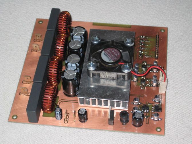
Scheme of the power stage shown in Fig. 8. Circuit TAS5611A it is taken from the manufacturer. The input stereo signal inputted to the connectors X10, X11 continues through the coupling members to the operational amplifier OPA1632. There is a transfer of unsymmetrical signal on the differential. The signal further via coupling members enters in the integrated circuit TAS5611A. Power PWM signal, protruding from the chip is conducted to the output of the filter formed by the elements of the L1X, C5X. Filter cut-off frequency has a value of 73kHz. The outputs of the amplifiers are provided with Boucherotovými members, consisting of a serial combination of the elements of the R7X and C7X.
![]() tas5611a class-d amplifier pcb schematic all files alternative links:
tas5611a class-d amplifier pcb schematic all files alternative links:
FILE DOWNLOAD LINK LIST (in TXT format): LINKS-25553.zip
Published: 2016/06/06 Tags: audio amplifier circuits, class d amplifier circuit, ic amplifier
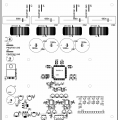
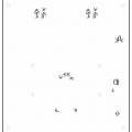
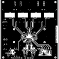
Audio Input Selector Circuit
The main parts of the switch inputs is the decimal counter CD4017. Resistors R5 and R6 serves to limit the input current to the counters and, together with capacitor C1 form the RC divider. His task is to prevent multiple switch, when pressing a button, the influence of mechanical oscillations of the contacts of the button. To the counter read, must be on pins ENA and reset log. 0. On the outputs 0 – 3 are connected resistors for limiting the current of the LED diode and transistorem. Transistory here have the function switch and operates relays, for which, at rest de-energized, the contacts is connected the input audio signal. When the switching transistor switches the position relay and connects to the output the appropriate input stereo signal.
TAS5611A Klasse-D Verstärker Schaltung Projekt
Das Blockschaltbild der integrierten Schaltung TAS5611A Wie oben erwähnt, die Schaltung enthält 4 identische Kanäle. Das Eingangssignal zugeführt wird pin INPUT_X. Das Signal setzt sich in der feedback-filter ANALOG LOOP FILTER und weiter an die Eingangs-multiplexer der ANALOG-EINGANGS-MUX. Im block ANALOG-KOMPARATOR MUX tritt zum vergleichen des Eingangssignals mit einer Referenzspannung. Das resultierende PWM-Signalverarbeitung PWM-RECEIVER. Gefolgt von der Prozedur signal im block STEUERUNG und timing des Signals in den block DER TIMING-STEUERUNG. Der Letzte block ist der Erreger power-transistoren mit GATE-ANTRIEB, der verbunden ist mit der pin BST_X. Diese TAS5611A pin dient der Verbindung mit einem “bootstrap” – Kondensator. Ein Hilfs-diode für die Verwaltung der Art, wie die “bootstrap” ist integriert in den chip. Macht die Spannung der halb-Brücken verbunden ist, der zwischen den pins PVDD_X und GND_X. Versorgungsspannung Logik-und Kontroll-Blöcke, die in der Schaltung geliefert wird, an pins für VDD und GVDD_X. Power-PWM-signal led out-pin OUT_X.