The circuit consists of the following units: a rectifier with a filter, a +12V voltage stabilizer, voltage stabilization, current stabilization, indication, a control unit and overheating protection. If the output voltage can reach 50V, and not limited to the supply voltage of the op-amp (32 V), as in the vast majority of LBP circuits. The stability of the device and its repeatability are just wonderful. Therefore, I recommend the reader to assemble this simple and inexpensive laboratory power supply for his home workshop.
The rectifier consists of a step-down transformer TV1, a diode bridge VDS1 and a filter C1.
The +12V voltage regulator is made on the basis of the VD1 microcircuit and on the VT1 transistor. Stabilized voltage + 12V is powered by the operational amplifier DA1. Also, this value is used as a reference voltage source in the adjustment nodes.
When the key S1 is closed, the power supply stops working in the current stabilization mode, and the trigger protection turns on (DA1.2 interacts with DA1.4), which, if the set threshold is exceeded, reduces the output current of the LBP to zero until the key S1 is broken.
The indication unit is made on the op-amp DA1.4, operating as a comparator that controls the glow of the HL1 and HL2 LEDs, depending on the stabilization mode (current or voltage). This node is not required, but it is very convenient for me to see the threshold for switching on the current stabilization mode when checking some devices.
As the temperature rises, the resistance R31 decreases and the potential increases at the inverse input DA1.3, and when it is greater than the potential at the direct input (set value using R34), then ground (GND) will appear at the output DA1.3. In this case, the HL3 LED will light up, the transistor VT3, and after it VT4 and VT2 will close.
0-50V Adjustable Power Supply Schematic
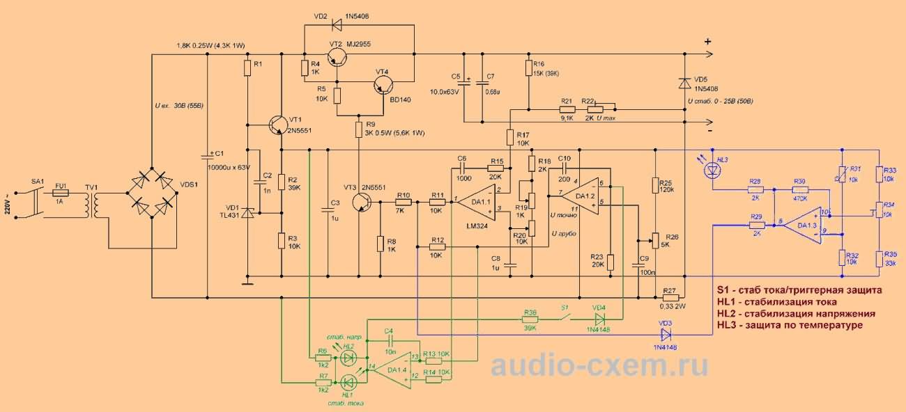
The control unit consists of two transistors VT2 and VT4, connected according to the circuit of a composite transistor to increase the gain. VT4 is the most loaded element. It dissipates a large amount of heat proportional to the difference between the input and output voltage when the load current flows through it. Transistors VT2 and VT4 are controlled by VT3.
As can be seen from the diagram, the transistor VT2 is direct conduction (PNP). Below is a circuit diagram for switching on an NPN reverse-conducting transistor. It is under such a structure (NPN) of the VT2 transistor that the printed circuit board is divorced (link under the article).
Chip DA1 is a quad operational amplifier LM324. All four channels are independent of each other. A feature of this op-amp is the presence of PNP transistors at its inputs. Therefore, when replacing the LM324, it is necessary to select an analog with the presence of bipolar PNP transistors at the input, and also so that the analog can provide an output zero bias voltage close to zero. The LM324 chip can be replaced with two LM358 chips (requires new PCB layout).
The diode bridge can be assembled from 1N5408 rectifier diodes or a ready-made bridge such as KBU610 or KBU810 can be used. The filter capacitance C1 (10,000 uF) when charging will provide a fairly large current through the bridge, this must be taken into account.
For the convenience of adjusting the output parameters of the power supply, it is necessary to use variable resistors R20 and R26 with a linear relationship. If you use potentiometers with a logarithmic dependence, then when you turn their knobs by the same angle, the resistance will change unevenly. This is especially noticeable if a uniform (linear) scale with digital values is drawn on the case.
Trimmer resistors R22 and R34 are better to use multi-turn type 3296W, they allow you to smoothly and conveniently configure the device. For R31 I used a 10kΩ NTC thermistor.
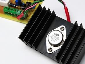
Transistor VT2 for the printed circuit board attached to the article must be NPN conductivity. Its rated collector current and Uke is selected with a margin. In addition, there must be a margin of dissipated power. So, with Uin=50V, Uout=3V and Iload=1.5A, the dissipated power on the transistor will be P=(50V-3V)×1.5A=71W. Which is quite a lot. For such a case, the transistor must be designed for a power dissipation of at least 100-120W and have good cooling (read below). I installed 2N3055 as VT2, you can put TIP35C or 2SC5200.
0-50V Power Supply Circuit Cooling
It is necessary to cool the VT2 case. The heat sink must be installed outside the power supply case for effective natural convection, or active (forced) cooling must be used. The radiator area for passive cooling is recommended to choose a calculation of 10-20cm 2 per 1W of the dissipated power of the transistor, which is equal to P \u003d (Uin-Uout) × Iload. If long-term work with a load is planned, then we take 20cm 2 per 1W, and if the LBP will be used only for checking or starting devices, then 10cm 2 per 1W can be dispensed with.
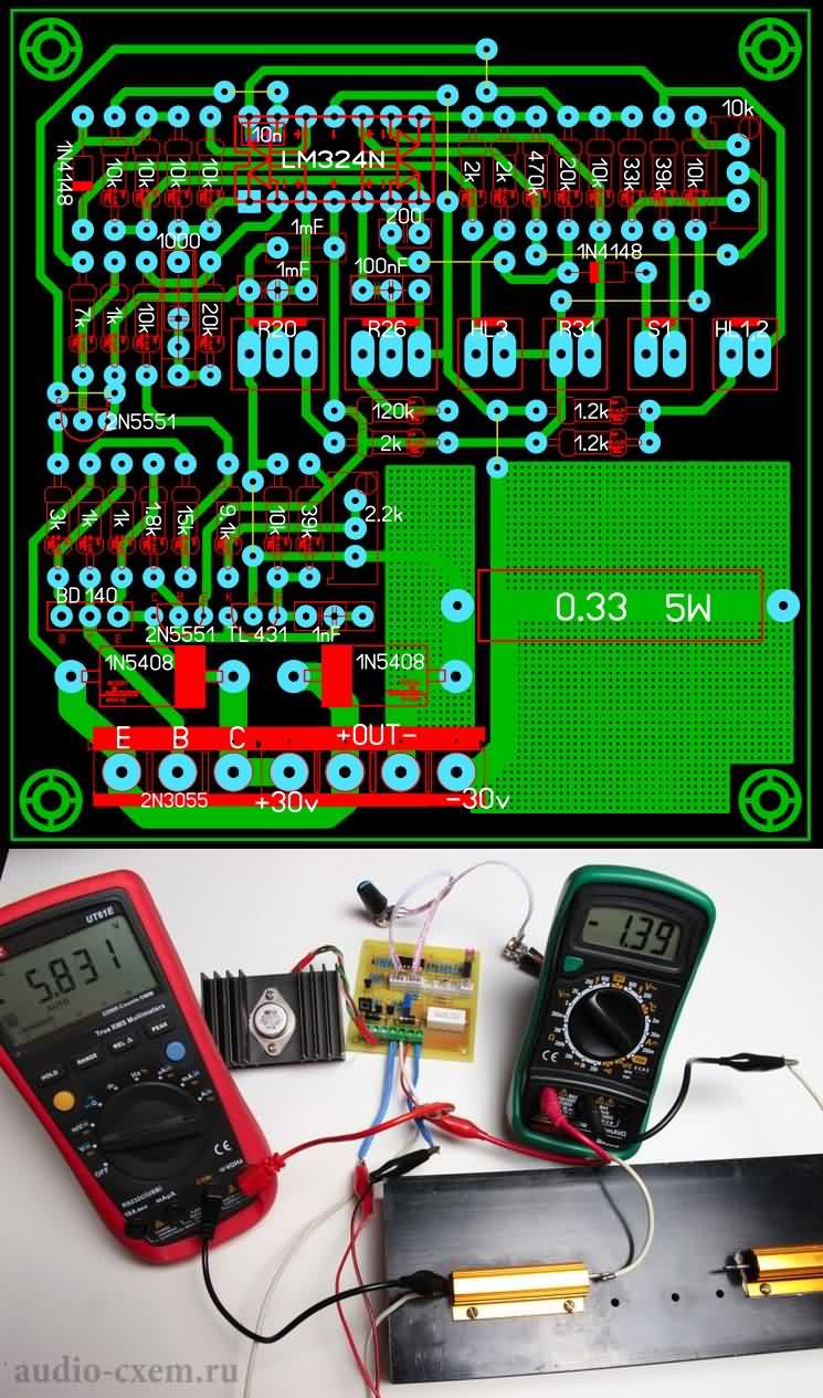
Alternate link for PCB, schematic files: 26756b.zip pass: 320volt.com
Source: audio-cxem.ru/shemyi/istochniki-pitaniya/laboratornye/prostoj-i-dostupnyj-blok-pitaniya-0-50v.html

من از مدارهایی که میگذارید مخصوصا مدارات تغذیه برای تحقیق استفاده میکنم