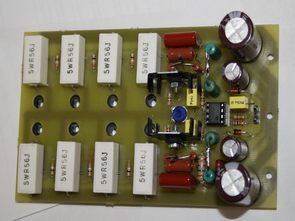
Despite the apparent simplicity, this amplifier showed excellent quality parameters, which allows you to safely rank it as a Hi-Fi equipment. The amplifier has a very pleasant sound in the mid-eighties was patented. Since then, the element base has changed quite a lot and it has been possible to simplify the circuit, preserving the idea itself and getting the best characteristics without compromising reliability.
The circuitry of the entire line of these amplifiers is almost the same, they differ only in the number of terminal transistors – in the MOSFIT-100 version, one pair is used, in the MOSFET-400W variant – 4 pairs.
The circuit has a preliminary buffer voltage amplifier made on the TL071 op amp and a two-stage push-pull power amplifier. The circuitry of the output stage is constructed in such a way that, in fact, it is two independent amplifiers – for the positive half-wave of the sound signal (VT1 – driver, VT3, VT5, VT7, VT9 – terminal transistors) and for the negative half-wave (VT2 – driver, VT4, VT6, VT8, VT10 – terminal transistors). Both amplifiers are covered by their local negative feedbacks: R13-R9 and R14-R10. The gain depends on the ratio of the ratings of these resistors, and in this case it is chosen in such a way as to obtain minimal distortion in this cascade.
Changing the ratings is not recommended (R9 and R10 can be from 27 to 43 Ohms, optimally – 33 or 39 Ohms). Since the last stage operates in the amplifier mode, entering the saturation mode, the resistance between the output of the amplifier and the power source becomes the minimum possible (0.2 – 0.5 Ohm). It is this factor that allows MOSFIT to have a much higher efficiency at the output compared to traditional amplifiers with emitter followers, since the amplitude of the output signal is only a few volts less than the supply voltage.
400W Amplifier Circuit schematic
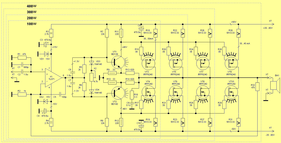
In addition to local negative feedback (OOS), the entire amplifier is covered by another OOS branch, consisting of R2 and R32. In this case, the gain is KU = R32 / R2 + 1 = 48 times (33 dB). Within small limits, you can change R2 to obtain the required gain, but do not exceed 37 dB (R2 should not be less than 680 Ohms) The list of elements necessary for self-assembly of the amplifier is summarized in the table below.
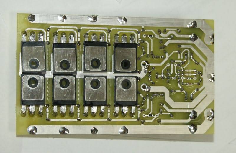
Terminal transistors are installed on the radiator through electrically insulating heat-conducting gaskets, having previously lubricated the flanges with heat-conducting paste. A “common” wire should be fed to the radiator. However, you can do without gaskets, but it should be borne in mind that the output signal of the amplifier will be present on the radiator, which can cause the excitation of the amplifier, the radiator must be isolated from the case. In fig. 2 shows a drawing of a printed circuit board and the location of parts on it.
Of the features of the amplifier, it should also be noted that the flanges of the terminal transistors are electrically connected between themselves and the output of the amplifier, so when using small heat sinks with forced cooling, you can not use dielectric gaskets, but rather isolate the radiator from the case. When using heat sinks with natural air convection, the dimensions of the latter already become large and it is not recommended to supply an amplifier output to it – too much interference will be created, which, if the boards are installed incorrectly in the case, can cause the amplifier to excite, even despite its rigid stability.
In fig. Figures 3 and 4 show voltage maps for a variant of a 200 W amplifier with a ± 45 V supply voltage and two pairs of terminal transistors and a 400 W amplifier with a ± 65 V supply voltage. Both variants are loaded on the speaker equivalent (yellow rectangle) and do not use ideal power supplies with their own resistance.
Voltage map of a 200 W power amplifier and ± 45V power supply
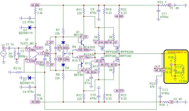
Voltage map of a 400 W power amplifier and ± 65V power supply
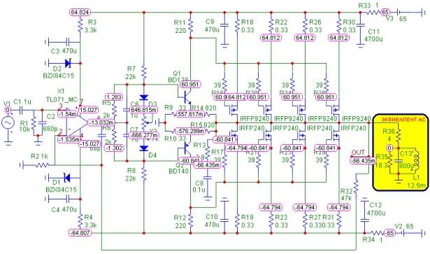
Perhaps it is worth noting that the model used IRF640-IRF9640 transistors, as the closest analogs to the IRFP240-IRFP9240, but with a lower power dissipation by the heat crystal, since they have a TO-220 housing against TO-247. Nevertheless, the IRF640-IRF9640 in the simulator completely coped with the tasks assigned to them, and can also be used in the amplifier as terminal transistors.
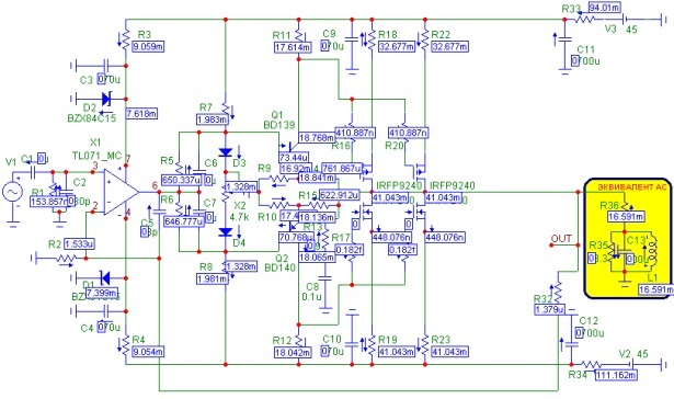
However, when using TO-220 cases, one should not forget that the power of one TO-220 case should not exceed 60 W, unlike the TO-247 case, up to 100 … 120 W. In other words, when using an IRF640-IRF9640 as a terminal transistor, it is not recommended to shoot more than 240 watts from an amplifier with four pairs. Figures 5 and 6 show maps of currents flowing through each element of the amplifier in standby mode (no input signal).
Current map of the power amplifier at a supply voltage of ± 45 V
Current map of the power amplifier at a voltage of ± 65V
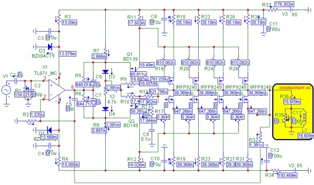
The quiescent current of the terminal stage should be set within 30-40 mA – this is quite enough for the complete disappearance of distortions of the “step” type and the technological reserve for increasing the supply voltage. This is worth mentioning separately: this amplifier does not have any current-stabilizing chains, therefore, when the supply voltage changes, the operating modes of the terminal stage will also change – with an increase in the supply, the quiescent current will increase, with a decrease, it will decrease.
This does not matter much if the mains voltage varies within 5% or a stabilized power supply is used for the amplifier, but if the mains voltage decreases by 10%, which happens quite often on the periphery, then a step is already guaranteed to appear on the amplifier output, and if increases by 10%, then the quiescent current will already be 0.45 A, and the power allocated to each transistor (when powered ± 65 V + 10% and four pairs of powerful transistors) will be about 30 W, which ultimately will cause heat generation of about 200 W, moreover, on ho Ost go!
For this reason, it is recommended to use the amplifier as a broadband with a high-quality supply voltage, or as an amplifier for a subwoofer and setting the quiescent current within 15 – 20 mA. With a decrease in power supply, the “step” that appears is a low-frequency dynamic head is simply not able to reproduce due to the inertia of the diffuser, and with an increase in the quiescent current it will remain within the permissible and such a strong heating of the heat sink will not occur.
As thermostabilizing elements, VD3-VD4 diodes are used, which can be installed both on the radiator and remain on the printed circuit board – instant heating does not occur anyway, therefore the heating speed of the board installed above the radiator is quite enough. Figure 7 shows the currents flowing in cascades at a temperature of 20 ° C, and in Figure 8 – at a temperature of 60 ° C, that is, with a temperature increase of 3 times.
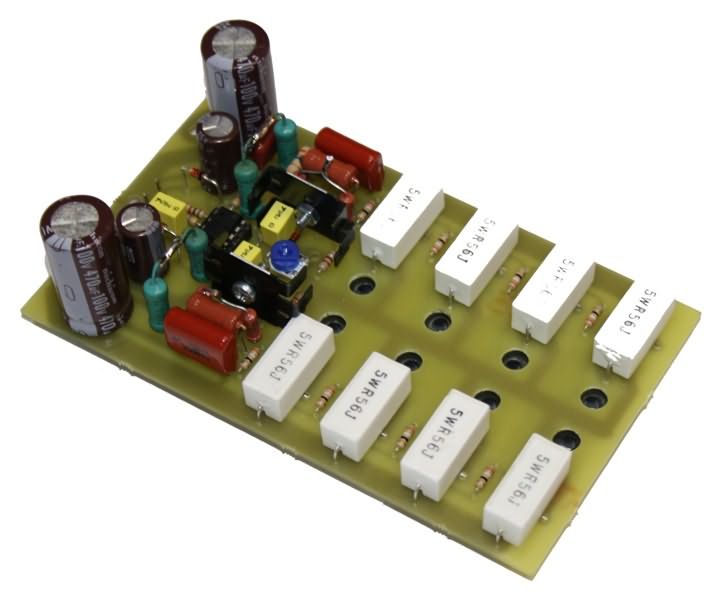
Update: A reader from India made the circuit as 200w with 4 mosfets, but it did not work. He said that it worked perfectly when he installed an LM741 op amp instead of TL071. The TL071 op amp should not have the same difference as the LM741, but I still wanted to let you know.
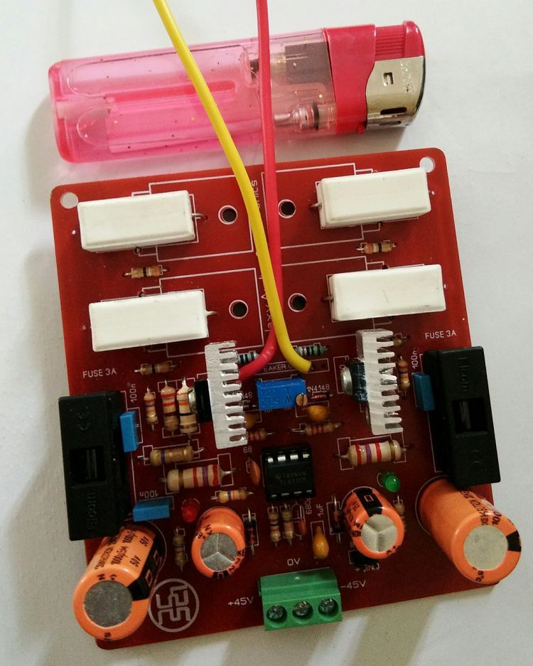
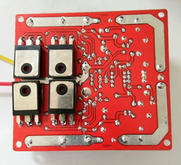
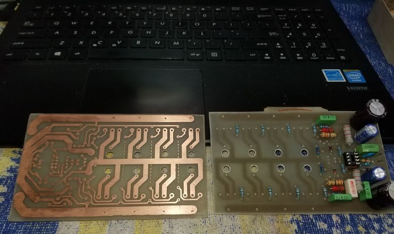
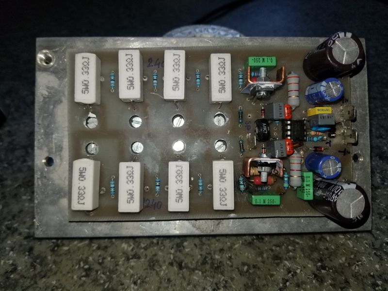
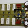
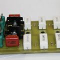
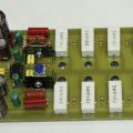
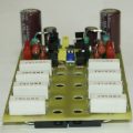
Update 22-05-2020: A reader from Macedonia made a 400w version of the circuit and ran it with 50v, said that it sounded very good and sent the pictures.
Şifre-Pass: 320volt.com
Source: mariolla.com/index.php/amplifier/34-stk442-090.html
Publication date: 2019/08/08 Tags: audio amplifier circuits, transistor amplifier
greetings, how to convert this amplifier to quasi?
Hi! Hope you’re doing well.
I would like to build a stereo anmplifier with two of this boards. I need a speaker protection circuit, do you know some schematic to recommend?
Thanks for this post.
Kind regards!
Hi,
https://320volt.com/en/speaker-protection-circuit/
Best regards.
hello and thank you very much but I have a question, in the schematic the resistor R7 is 22k but on the board it is 27k. Which is the right one? Also on the board there is capacitor on the positive and negative voltage line which then goes to the ground which have no value.thank you very much
https://ibb.co/QDD0bbj
Hi,
R7 you can use 27k. Capacitors 100nf 50v….100v (according to the operating voltage of the circuit)
thank you very much
Hi good day to you
can i change irfp9240 to 2sa19430 and irfp 240 to 2sc5200 i’m working with 65 v
Sorry about multi reply due to first time visit 320Volt.com
The battery-powered fully modular amplifier I designed also uses a similar power amplifier architecture.
However, I replaced the BD139/140 driver stage with an LT1085 as a cross-current source and an OP base analog adder.
All OP use the AD815, which is originally used for driving ADSL transformers. Additionally, a DC-SERVO circuit is incorporated.
This circuit work perfectly with +/- 14.75V Battery supply to drive my TANNOY GRF Memory speaker (15″ coaxial horn speaker unit)
https://images.plurk.com/3DMyOJrRCz2ux4wuj7ujR5.png
https://images.plurk.com/5hRX2k1E2aiLCaK5MR7aNr.png
https://images.plurk.com/4L74vfbrFVItLvFGsPx1Dn.jpg
https://images.plurk.com/1mbb7cxOxD2ifShYXGCD9E.jpg
https://images.plurk.com/1zEhnlye7EapzcWDkqj5hu.jpg
https://images.plurk.com/5twPLfQ4AOhNbWJjFLvivL.jpg
https://images.plurk.com/26KFQe0meUMJYa3pYyKsRQ.jpg
https://images.plurk.com/brJa82BA6TlpkbFy3tpwe.jpg
https://images.plurk.com/3uTaiQipTeGY15gAIThvJC.jpg
https://images.plurk.com/2R4BDmK1faeYQvCHYB60mB.jpg
Hi everyone, I built a mosfit-100 (this is for testing, because I am building 2×200 and 1×200 for a subwoofer) it worked very well and the sound is great, both high and low frequencies 👌👌👌 in general everything works great,
Question, does this amp work without acoustic protection? Please explain in more detail
Hi everyone! If I add a couple of transistors, will this amp handle up to 1000W?