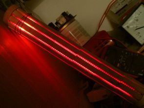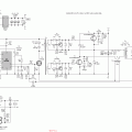
This switching power supply was created because I needed a controllable laboratory power source for more power. A linear topology would be unusable for this power (2400W). So I chose the topology of a single-acting leaky power supply with two switches, or a half-bridge. In my article on resources , it’s a topology II.D. Power supply uses IGBT transistors and is controlled by UC3845. The line voltage first passes through the EMC filter. It is then rectified by a bridge and filtered on C4 capacitors. To limit the current surge, a step switch with Re1 and R2 is connected in the way. The relay coil and fan (from an AT / ATX PC power supply) are powered from 12V, which is obtained by shrinking from the 17V auxiliary power supply. Select R1 so that the relay and fan coil voltage is 12V. The auxiliary power supply uses the TNY267 circuit. It is similar to the resource described here.
R27 provides undervoltage protection of the auxiliary power supply – it does not switch on at less than 230V DC. The UC3845 control circuit has a frequency of 50kHz and a maximum duty cycle of 47%. It is powered via a zener diode, which reduces the supply voltage by 5.6V (ie to 11.4V) and also shifts the UVLO thresholds from 7.9V (lower) and 8.5V (upper) to 13.5V and 14.1V. Thus, the power supply will start operating at 14.1V and will never run below 13.5V, protecting the IGBT from desaturation. The original UC3845 thresholds were set too low. The circuit is controlled by the MOSFET T2, which controls the pass-through transformer Tr2. This ensures galvanic separation and floating excitation. Through the T3 and T4 forming circuits, IGBT gates trigger T5 and T6. These switch the rectified mains voltage (325V) to the power transformer Tr1. Its output is then rectified by a permeable rectifier and smoothed by L1 choke and capacitors C17. Voltage feedback It is applied from the output to the 2nd terminal of IO1. The voltage can be adjusted using the potentiometer P1. Galvanic feedback is not necessary because the control circuit is connected to the secondary side of the power supply and separated from the mains. The current feedback is applied through the current transformer Tr3 to the third terminal IO1. The current protection threshold can be set with P2.
Transistors T5 and T6, diodes D5, D5 ‘, D6, D6’, D7, D7 ‘, and the bridge must be placed on the heatsink. D7 diodes, C15 capacitors, and R22 + D8 + C14 protective RDC cells should be located as close as possible to the IGBT. LED 1 indicates power on, LED 2 indicates current mode or fault. Lights up when the power supply is not operating in voltage mode. In voltage mode, the output is 1 IO1 2.5V, otherwise it is about 6V. LED indicators can be omitted.
Inductances: I used the transformer Tr1 from the old 56V power source. The primary to secondary transformation ratio is about 3: 2 to 4: 3 and the core is ferrite EE without air gap. If you would like to wind it yourself, use a similar core as in my welding inverter , ie approx. 6.4cm2 (acceptable range is 6-8cm2). Wrap 20z 20 wires of 0.5 – 0.6mm diameter on the primary and 14z 28 wires of the same diameter on the secondary. Winding with copper strips is also possible. Conversely, the use of a single thick conductor is not possible due to the surface phenomenon (working at high frequencies). It is not necessary to divide the windings, eg wind the primary and then the secondary. The excitation transformer Tr2 has three windings of 16 turns each. They are wound all at once (trifilarly) by three spiral coiled insulated bell wires. It is wound on ferrite core EI (can be EE) without air. gaps from power transformer from PC power supply ATX, event. AT. The core has a cross-section of the central pillar of approx. The current transformer Tr3 has 1z and 68z on the ferrite ring and the size and number of turns is not critical. For a different number of turns, adjust R15. The transformer of the auxiliary power supply Tr4 is wound on a ferrite EE core with an air gap and cross-section of the center post of approx. 16 – 25mm2. It comes from transformer auxiliary gutted ATX. The winding orientation of all transformers (marked by dots) must be observed. The double line filter choke can be, for example, a microwave. The output choke L1 also comes from a 56V power supply. It consists of two parallel chokes 54uH on the iron-dust rings and the total inductance is therefore 27uH. Each choke is wound with two lacquered copper wires 1.7mm. The total conductor cross-section is approx. 9mm2.
L1 is connected to the negative branch so that there is no RF voltage on the cathode of the diodes and can be mounted on the heatsink (or part thereof) without insulation. Maximum power consumption is about 2600W and efficiency at full load more than 90%. I used IGBT type STGW30NC60W. They can be replaced, for example, by the IRG4PC40W, IRG4PC50W, IRG4PC50U, STGW30NC60WD or similar sufficiently powerful and fast. The output diodes can be any fast with sufficient current. The upper diodes (D5) see the mean current at most 20A, the lower diodes (D6) the most at 40A. Thus, the upper diodes can be designed for half current than the lower ones. For example, the upper diodes may be two HFA25PB60 / DSEI30-06A or one DSEI60-06A / STTH6010W / HFA50PA60C. The bottom may be two DSEI60-06A / STTH6010W / HFA50PA60C or four HFA25PB60 / DSEI30-06A. The heatsink of the diodes must allow for a loss of approx. The IGBT loss can be up to 50W together. The loss of D7 is difficult to estimate because it depends on the properties of Tr1 (inductance and scattering). Loss of bridge is up to 25W. The power supply uses a similar circuit as the welding inverter because it has worked well. Switch S1 allows stand-by switching off the power supply because frequent switching off of such a high-power supply by the mains switch would not be suitable (especially when used as a laboratory power supply). Power consumption in the off state is only about 1W. S1 can be omitted. The power supply can also be built as a fixed voltage source. In this case, it is advisable to optimize the transform ratio Tr1 for best efficiency (eg, a primary 20z and a secondary 1z for each 3.5-4V).
Attention! The pulse source is not intended for beginners because most of its circuits are connected to the network. In the case of poor construction, the mains voltage can reach its output! The output voltage may exceed the safe contact voltage. It is a source of high power that needs to be adequately protected. It is also necessary to sufficiently dimension the power supply. Capacitors can remain charged even after switching off. Everything you do at your own risk, for any injury or property I do not take responsibility.
Source: danyk.wz.cz/reg60v.html alternative link:
FILE DOWNLOAD LINK LIST (in TXT format): LINKS-18270.zip
Publication date: 2012/01/03 Tags: power electronic projects, smps circuits, smps projects, smps schematic

PLCC CQFP DIP Converter PCB
In experiments with a variety of microcontrollers to PLCC CQFP hard devresinizi design and begin to implement completely integrated direct pcb and holding down the mount and a converter card output or pinleriden you’re going to start over attempts to Mohammed bord and so the second option is more appropriate converter can be used to integrate a lot of various sizes of card printing circuit of universal.