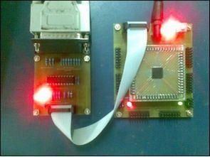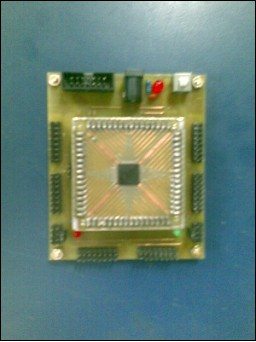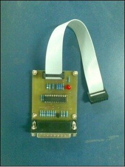
MSP430f149 prepared for the parallel port JTAG Programmer circuit of the circuit diagram, pcb (protel and pdf)’s.


MSP430F Features
Low Supply Voltage Range, 1.8V . . . 3.6V
Ultra-Low Power Consumption:
Active Mode: 280 µA @ 1 MHz, 2.2V
Standby Mode: 1.6 µA
Off Mode (RAM Hold): 0.1 µA
Five Power Saving Modes
Wake Up from Standby Mode in Less Than 6 µs
16-Bit RISC Architecture, 125-ns Instruction Cycle Time
12-Bit A/D Converter with Internal Reference, Sample-and-Hold, and Autoscan
16-Bit Timer_B with Seven Capture/Compare Registers
16-Bit Timer_A with Three Capture/Compare Registers
On-Chip Comparator
Serial Onboard Programming, No External Programming Voltage Required Programmable Code Protection with Safety Fuse
Serial Communication Interface (USART) Functions as Asynchronous UART or Synchronous SPI Interface
Two USARTs (USART0, USART1) — MSP430x14x(1) Devices
One USART (USART0) — MSP430x13x Devices
MSP430F133: 8KB+256B Flash Memory, 256B RAM
MSP430F135: 16KB+256B Flash Memory, 512B RAM
MSP430F147, MSP430F1471: 32KB+256B Flash Memory, 1KB RAM
MSP430F149-JTAG
The Texas Instruments MSP430 ultra-low power microcontroller family consists of several devices with different peripheral sets targeted for various applications. Combined with five low power modes, the architecture is optimized to achieve longer battery life in portable measurement applications. The device features a powerful 16-bit RISC CPU, 16-bit registers, and fixed generators attributed to maximum code efficiency. The digitally controlled oscillator (DCO) allows wake-up from low-power modes to active mode in less than 6 µs.
The MSP430x13x and MSP430x14x(1) series are microcontroller configurations that include two internal 16-bit timers, a fast 12-bit A/D converter (not implemented in the MSP430F14x1 devices), one or two universal serial synchronous/asynchronous communication interfaces (USART), and 48 I/O pins.
MSP430f149 JTAG schematic pcb files:
Şifre-Pass: 320volt.com
Publication date: 2010/07/24 Tags: microcontroller projects, msp430 projects, programmer circuit
DAC Circuit CS8416 CS4398
Digital audio applications have not done anything but CS8416 (192 kHz Digital Audio Receiver) and CS4398 (CS4398: 120 dB, 24-Bit, 192 kHz Stereo D / A Converter) integrated carried out with the DAC module circuitry of the person concerned may be useful to PCB drawing is so much quality
What is the DAC?
DAC, DAC or D-to-A (Digital to Analog Converter) that can be translated into our language as digital-to-analog converter is a special identification. Especially since the emergence of the CD, the media having the recorded data due to digital data converted into analog has been used for the purpose. Mounted into the chassis of a CD player, although as will be used as a separate device. In particular, appears in separate use professional equipment. The purpose of the CD reading mechanisms of mechanical vibrations and other electronic components inside the device during the digital to analog conversion is to minimize interaction. With different technologies, though, CD, SACD, DVD-like digital recording platforms all used to do