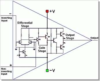
Opamplar hakkında çok detaylı (ingilizce) bir kaynak bir çok örnek uygulama bulunuyor filtre, amplifikatör, osilatör, geri besleme tasarımları en ince detayına kadar hesapmala bilgileri formüller.
Ayrıca devre ve pcb tasarımı hakkında dikkat edilecek bölümler hakkında bilgilerde bulunuyor özellikle formüller ve benzetimler işinize yarayabilir.

İçerik;
The Op Amp’s Place In The World
Review of Circuit Theory
Introduction
Laws of Physics
Voltage Divider Rule
Current Divider Rule
Thevenin’s Theorem
Superposition
Calculation of a Saturated Transistor Circuit
Transistor Amplifier
Development of the Ideal Op Amp Equations
Ideal Op Amp Assumptions
The Noninverting Op Amp
The Inverting Op Amp
The Adder
The Differential Amplifier
Complex Feedback Networks
Video Amplifiers
Capacitors
Single Supply Op Amp Design Techniques
Single Supply versus Dual Supply
Circuit Analysis
Simultaneous Equations
Case 1: VOUT = +mVIN+b
Case 2: VOUT = +mVIN – b
Case 3: VOUT = –mVIN + b
Case 4: VOUT = –mVIN – b
Feedback and Stability Theory
Why Study Feedback Theory?
Block Diagram Math and Manipulations
Feedback Equation and Stability
Bode Analysis of Feedback Circuits
Loop Gain Plots are the Key to Understanding Stability
The Second Order Equation and Ringing/Overshoot Predictions
References
Development of the Non Ideal Op Amp Equations
Introduction
Review of the Canonical Equations
Noninverting Op Amps
Inverting Op Amps
Differential Op Amps
Voltage-Feedback Op Amp Compensation
Introduction
Internal Compensation
External Compensation, Stability, and Performance
Dominant-Pole Compensation
Gain Compensation
Lead Compensation
Compensated Attenuator Applied to Op Amp
Lead-Lag Compensation
Comparison of Compensation Schemes
Conclusions
Current-Feedback Op Amp Analysis
CFA Model
Development of the Stability Equation
The Noninverting CFA
The Inverting CFA
Stability Analysis
Selection of the Feedback Resistor
Stability and Input Capacitance
Stability and Feedback Capacitance
Compensation of CF and CG
Voltage- and Current-Feedback Op Amp Comparison
Introduction
Precision
Bandwidth
Stability
Impedance
Equation Comparison
Op Amp Noise Theory and Applications
Characterization
rms versus P-P Noise
Noise Floor
Signal-to-Noise Ratio
Multiple Noise Sources
Noise Units
Types of Noise
Shot Noise
Thermal Noise
Flicker Noise
Burst Noise
Avalanche Noise
Noise Colors
White Noise
Pink Noise
Red/Brown Noise
Op Amp Noise
The Noise Corner Frequency and Total Noise
The Corner Frequency
Op Amp Circuit Noise Model
Inverting Op Amp Circuit Noise
Noninverting Op Amp Circuit Noise
Differential Op Amp Circuit Noise
Putting It All Together
Understanding Op Amp Parameters
Operational Amplifier Parameter Glossary
Additional Parameter Information
Input Offset Voltage
Input Current
Input Common Mode Voltage Range
Differential Input Voltage Range
Maximum Output Voltage Swing
Large Signal Differential Voltage Amplification
Input Parasitic Elements
Output Impedance
Common-Mode Rejection Ratio
Supply Voltage Rejection Ratio
Supply Current
Slew Rate at Unity Gain
Equivalent Input Noise
Total Harmonic Distortion Plus Noise
Unity Gain Bandwidth and Phase Margin
Settling Time
Instrumentation: Sensors to A/D Converters
Transducer Types
Design Procedure
Review of the System Specifications
Reference Voltage Characterization
Transducer Characterization
ADC Characterization
Op Amp Selection
Amplifier Circuit Design
Wireless Communication: Signal Conditioning for IF Sampling
Wireless Systems
Selection of ADCs/DACs
Factors Influencing the Choice of Op Amps
Anti-Aliasing Filters
Communication D/A Converter Reconstruction Filter
External Vref Circuits for ADCs/DACs
High-Speed Analog Input Drive Circuits
Interfacing D/A Converters to Loads
Introduction
Load Characteristics
DC Loads
AC Loads
Understanding the D/A Converter and its Specifications
Types of D/A Converters — Understanding the Tradeoffs
The Resistor Ladder D/A Converter
The Weighted Resistor D/A Converter
The R/2R D/A Converter
The Sigma Delta D/A Converter
D/A Converter Error Budget
Accuracy versus Resolution
DC Application Error Budget
AC Application Error Budget
RF Application Error Budget
D/A Converter Errors and Parameters
DC Errors and Parameters
AC Application Errors and Parameters
Compensating For DAC Capacitance
Increasing Op Amp Buffer Amplifier Current and Voltage
Current Boosters
Voltage Boosters
Power Boosters
Single-Supply Operation and DC Offsets
Sine Wave Oscillators
What is a Sine Wave Oscillator?
Requirements for Oscillation
Phase Shift in the Oscillator
Gain in the Oscillator
Active Element (Op Amp) Impact on the Oscillator
Analysis of the Oscillator Operation (Circuit)
Sine Wave Oscillator Circuits
Wien Bridge Oscillator
Phase Shift Oscillator, Single Amplifier
Phase Shift Oscillator, Buffered
Bubba Oscillator
Quadrature Oscillator
Conclusion
Active Filter Design Techniques
Fundamentals of Low-Pass Filters
Butterworth Low-Pass FIlters
Tschebyscheff Low-Pass Filters
Bessel Low-Pass Filters
Quality Factor Q
Low-Pass Filter Design
First-Order Low-Pass Filter
Second-Order Low-Pass Filter
Higher-Order Low-Pass Filters
High-Pass Filter Design
First-Order High-Pass Filter
Second-Order High-Pass Filter
Higher-Order High-Pass Filter
Band-Pass Filter Design
Second-Order Band-Pass Filter
Fourth-Order Band-Pass Filter (Staggered Tuning)
Band-Rejection Filter Design
Active Twin-T Filter
Active Wien-Robinson Filter
All-Pass Filter Design
First-Order All-Pass Filter
Second-Order All-Pass Filter
Higher-Order All-Pass Filter
Practical Design Hints
Filter Circuit Biasing
Capacitor Selection
Component Values
Op Amp Selection
Filter Coefficient Tables
Circuit Board Layout Techniques
General Considerations
The PCB is a Component of the Op Amp Design
Prototype, Prototype, PROTOTYPE!
Noise Sources
PCB Mechanical Construction
Materials — Choosing the Right One for the Application
How Many Layers are Best?
Board Stack-Up — The Order of Layers
Grounding
The Most Important Rule: Keep Grounds Separate
Other Ground Rules
A Good Example
A Notable Exception
The Frequency Characteristics of Passive Components
Resistors
Capacitors
Inductors
Unexpected PCB Passive Components
Decoupling
Digital Circuitry — A Major Problem for Analog Circuitry
Choosing the Right Capacitor
Decoupling at the IC Level
Decoupling at the Board Level
Input and Output Isolation
Packages
Through-Hole Considerations
Surface Mount
Unused Sections
Board Structure
Components
Routing
Bypass
Designing Low-Voltage Op Amp Circuits
Introduction
Dynamic Range
Signal-to-Noise Ratio
Input Common-Mode Range
Output Voltage Swing
Shutdown and Low Current Drain
Single-Supply Circuit Design
Transducer to ADC Analog Interface
DAC to Actuator Analog Interface
Comparison of Op Amps
A Single-Supply Circuit Collection
Introduction
Boundary Conditions
Amplifiers
Inverting Op Amp with Noninverting Positive Reference
Inverting Op Amp with Inverting Negative Reference
Inverting Op Amp with Noninverting Negative Reference
Inverting Op Amp with Inverting Positive Reference
Noninverting Op Amp with Inverting Positive Reference
Noninverting Op Amp with Noninverting Negative Reference
Noninverting Op Amp with Inverting Negative Reference
Noninverting Op Amp with Noninverting Positive Reference
Differential Amplifier
Differential Amplifier With Bias Correction
High Input Impedance Differential Amplifier
High Common-Mode Range Differential Amplifier
High-Precision Differential Amplifier
Simplified High-Precision Differential Amplifier
Variable Gain Differential Amplifier
T Network in the Feedback Loop
Buffer
Inverting AC Amplifier
Noninverting AC Amplifier
Computing Circuits
Inverting Summer
Noninverting Summer
Noninverting Summer with Buffers
Inverting Integrator
Inverting Integrator with Input Current Compensation
Inverting Integrator with Drift Compensation
Inverting Integrator with Mechanical Reset
Inverting Integrator with Electronic Reset
Inverting Integrator with Resistive Reset
Noninverting Integrator with Inverting Buffer
Noninverting Integrator Approximation
Inverting Differentiator
Inverting Differentiator with Noise Filter
Oscillators
Basic Wien Bridge Oscillator
Wien Bridge Oscillator with Nonlinear Feedback
Wien Bridge Oscillator with AGC
Quadrature Oscillator
Classical Phase Shift Oscillator
Buffered Phase Shift Oscillator
Bubba Oscillator
Triangle Oscillator
B Single-Supply Op Amp Selection Guide
Kaynak pdf dosyası: http://focus.ti.com/lit/an/slod006b/slod006b.pdf
Şifre-Pass: 320volt.com
Yayım tarihi: 2010/02/09 Etiketler: op-amp, opamp, opamp devresi, opamp hesaplama, Texas Instruments

eviren opampda pozitif referans ile ölçüm nasıl yapabilirim diye çabalayıp duruyordum. Bu paylaştığınız dosyada tam istediğim şey “Inverting Op Amp with Inverting Positive Reference” adında gösteriliyor.
Çok teşekkür ederim…