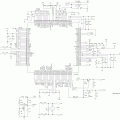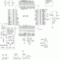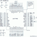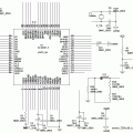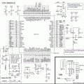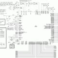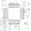
Günümüzde sık kullanılan Mp3, mp4 gibi ses video oynatıcı cihazların devrelerinde bulunan çok fonksiyonlu (ses kodek, video kodek tft lcd sürücülü vs..) multimedya entegre datasheet bilgileri bağlantı şemaları özellikle teknik servislerde tamir işleri için çok işe yarayabilecek şemalar bağlantı bilgileri bulunuyor.
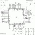
ATJ2180 pin out bağlantı şeması
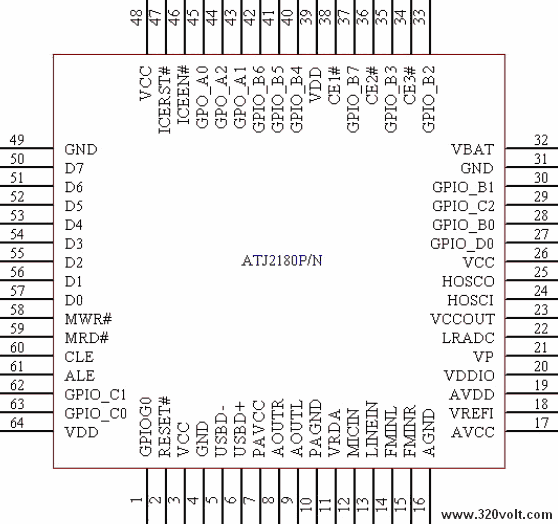
ATJ2180-pinout-schematic ATJ2180 datsheet, ATJ2180, ATJ2180 schematic
Avid A1569 Flash Media Player FM Transmitter Datasheet
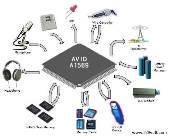
A1569 integrates high bandwidth USB2.0 for 480 mbps transfer rate. With high bandwidth, user can easily download music and upload voice recordings within minutes. Firmware can be upgradeable from USB port. For storage, NAND-type Flash is supported. It can support with 8-bit, 16-bit data bus width NAND Flash or it can use 2 pieces 8-bit NAND Flash to achieve high bandwidth. It can use up to 4 pieces to expand memory storage capacity. 8 bit Error detection and correction is generated for on board NAND Flash. A1569 supports card reader function for SD/MMC card. MP3(up to 384Kbps), MP2, WMA(up to 320Kbps) and ASF
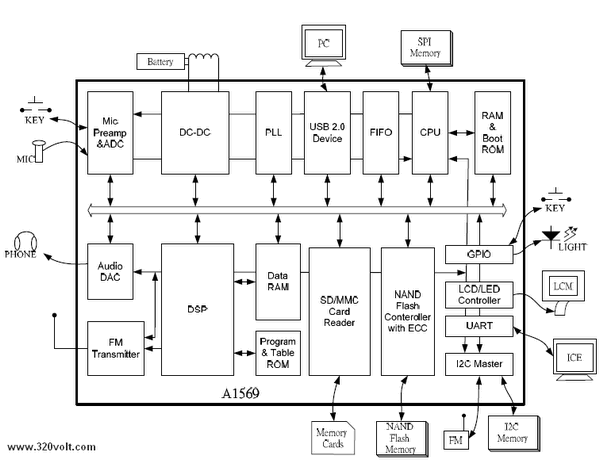
Pin Configuration LQFP Package
| Pin Number | Pin Name | Attrib. | Description |
|---|---|---|---|
| 1 | HPVDD | ANA | Headphone power |
| 2 | HPRINN | ANA | Headphone Right Channel In |
| 3 | HPLINN | ANA | Headphone Left Channel In |
| 4 | HPBYP | ANA | Headphone Bypass Capacitor |
| 5 | AVCC3 | ANA | DAC Power Supply |
| 6 | AVRC1 | ANA | DAC Voltage Reference Capacitor |
| 7 | LOUT | ANA | DAC Left Channel Out |
| 8 | COUT | ANA | DAC Voltage Reference Capacitor |
| 9 | ROUT | ANA | DAC Right Channel Out |
| 10 | AVRC2 | ANA | Reference bias capacitor |
| 11 | AGND3 | ANA | DAC Ground |
| 12 | GNDAD | ANA | Key scan & Voice Recording Ground |
| 13 | CVTI | ANA | ADC Top reference voltage |
| 14 | OPT1 | ANA | ADC Optional Channel 1 In |
| 15 | OPT2 | ANA | ADC Optional Channel 2 In |
| 16 | VDDAD | ANA | Key scan & Voice Recording Power |
| 17 | MICN | ANA | Mic positive input |
| 18 | MICP | ANA | Mic negative input |
| 19 | VDDMIC | ANA | MIC regulated power(3.3 to 2.8) |
| 20 | TVDD18D | ANA | Linear regulator 1.8V output |
| 21 | TVDD33R | ANA | Linear regulator 3.3V output |
| 22 | TVSS33R | ANA | Linear regulator Ground |
| 23 | HTVDD50 | ANA | USB 5V power |
| 24 | X1 | ANA | 32.768 K OSC |
| 25 | X2 | ANA | 32.768K OSC |
| 26 | VPOUT | ANA | RTC /Ring OSC power |
| 27 | VBY | ANA | Battery in |
| 28 | VSSDC | ANA | DC2DC analog ground |
| 29 | SHDN_SOC | ANA | DC2DC Hi enable power down and output will be pull low to zero |
| 30 | CP18 | ANA | Compensation connection |
| 31 | FB18 | ANA | DC2DC feedback |
| 32 | VOUT18 | ANA | DC2DC 1.8V output |
| 33 | PGND18 | ANA | DC2DC 1.8V driver Ground |
| 34 | LX18 | ANA | Connection to the external inductor for 1.8V |
| 35 | LX33 | ANA | Connection to the external inductor for 3.3V |
| 36 | PGND33 | ANA | DC2DC driver Ground |
| 37 | VOUT33 | ANA | DC2DC output |
| 38 | FB33 | ANA | DC2DC feedback |
| 39 | CP33 | ANA | Compensation connection |
| 40 | VSSCO | PWR | Digital Core Ground |
| 41 | VDDCO | PWR | Digital Core Power Supply |
| 42 | SEG27/GPIO7 | ANA/I/O | (1) LCM SEGMENT27 (2)GPIO port 7 |
| 43 | SEG26/GPIO4 | ANA/I/O | (1)LCM SEGMENT DATA26(2)GPIO port 4 |
| 44 | SEG25/GPIO5 | ANA/I/O | (1) LCM SEGMENT DATA25(2)GPIO port 5 |
| 45 | SEG24/FLCE2#/GPIO24 | ANA/I/O | (1) LCM SEGMENT DATA24(2)Flash Memory Chip Enable 2; (3) GPIO port 24 |
| 46 | SEG23/FLCE3#/GPIO23 | ANA/I/O | (1) LCM SEGMENT DATA23(2)Flash Memory Chip Enable 3; (2) GPIO port 23 |
| 47 | VSSIO | PWR | Digital IO Ground |
| 48 | SEG22/FLRB1#/GPIO22 | ANA/I/O | (1) LCM DATA22(2) Flash Memory Ready/Busy input 1; (2) GPIO port 22 |
| 49 | SEG21/GPIO21 | ANA/I/O | (1) LCM SEGMENT DATA 21 (2) GPIO port 21 |
| 50 | SEG20/GPIO20 | ANA/I/O | (1) LCM SEGMENT DATA20 (2) GPIO port 20 |
| 51 | SEG19/LCCS#/GPIO19 | ANA/I/O | (1) LCM SEGMENT DATA 19 (2) LCM Chip Select (3) GPIO port 19 |
| 52 | SEG18/LCA0/GPIO18 | ANA/I/O | (1) LCM SEGMENT DATA 18 (2) LCM Address 0 (3) GPIO port 18 |
| 53 | SEG17/LCSI/GPIO17 | ANA/I/O | (1) LCM SEGMENT DATA 17 (2) LCM Serial Data (3) LCM Read Enable (Intel) (4) LCM Enable (Motorola)(5)GPIO17 |
| 54 | SEG16/LCSCL/GOIP16 | ANA/I/O | (1) LCM SEGMENT DATA 16 (2) LCM Serial Clock (3) LCM Write Enable (Intel) (4) LCM R/W# (Motorola)(5)GPIO16 |
| 55 | VDDIO | PWR | Digital IO Power Supply |
| 56 | SEG15//FLD15/UA15/GPIO15 | ANA/I/O | (1) LCM SEGMENT DATA15(2) FLASH DATA15 (3) 8051 Address 15 (4) GPIO port 15 |
| 57 | SEG14/FLD14/UA14/GPIO14 | ANA/I/O | (1) LCM SEGMENT DATA 14(2) FLASH DATA14(3) 8051 |
| Address 14 (4) GPIO port 14 | |||
| 58 | SEG13/FLD13/UA13 | ANA/I/O | (1) LCM SEGMENT DATA 13(2) FLASH DATA13(3) 8051 Address 13 (4) GPIO port 13 |
| 59 | SEG12/FLD12/UA12 | ANA/I/O | (1) LCM SEGMENT DATA 12(2) FLASH DATA12(3) 8051 Address 12 (4) GPIO port 12 |
| 60 | SEG11/FLD11/UA11 | ANA/I/O | (1) LCM SEGMENT DATA 11(2) FLASH DATA11(3) 8051 Address 11 (4) GPIO port 11 |
| 61 | SEG10/FLD10/UA10 | ANA/I/O | (1) LCM SEGMENT DATA 10(2) FLASH DATA10(3) 8051 Address 10 (4) GPIO port 10 |
| 62 | SEG9/FLD9/UA9 | ANA/I/O | (1) LCM SEGMENT DATA 9(2) FLASH DATA9(3) 8051 Address 9 (4) GPIO port 9 |
| 63 | SEG8/FLD8/UA8 | ANA/I/O | (1) LCM SEGMENT DATA 8(2) FLASH DATA8(3) 8051 Address 8 (4) GPIO port 8 |
| 64 | VSSIO | PWR | Digital IO Ground |
| 65 | VLCD | PWR | LCD Power REFERENCE 5V TOLERENCE |
| 66 | SEG7/UAD7 | ANA/I/O | (1) LCM SEGMENT DATA 7 (2)8051 Address/Data 7 |
| 67 | SEG6/UAD6 | ANA/I/O | (1) LCM SEGMENT DATA 6 (2)8051 Address/Data 6 |
| 68 | SEG5/UAD5 | ANA/I/O | (1) LCM SEGMENT DATA 5 (2) 8051 Address/Data 5 |
| 69 | SEG4/UAD4 | ANA/I/O | (1) LCM SEGMENT DATA 4 (2)8051 Address/Data 4 |
| 70 | SEG3/UAD3 | ANA/I/O | (1) LCM SEGMENT DATA3 (2)8051 Address/Data 3 |
| 71 | SEG2/UAD2 | ANA/I/O | (1) LCM SEGMENT DATA 2 (2) 8051 Address/Data 2 |
| 72 | SEG1/UAD1 | ANA/I/O | (1) LCM SEGMENT DATA 1 (2)8051 Address/Data 1 |
| 73 | SEG0/UAD0 | ANA/I/O | (1) LCM SEGMENT DATA 0 (2)8051 Address/Data 0 |
| 74 | COM3/URE# | ANA/O | (1) LCD COMMON DATA 3 (2)8051 Read Enable |
| 75 | COM2/UALE | ANA/O | (1) LCD COMMON DATA 2 (2)8051 Address Latch Enable |
| 76 | COM1/UWE# | ANA/O | (1) LCD COMMON DATA 1 (2)8051 Write Enable |
| 77 | COM0/ROMOE# | ANA/O | (1) LCD COMMON DATA 0 (2) 8051 External ROM Output Enable |
| 78 | VSSCO | PWR | Digital Core Ground |
| 79 | VDDCO | PWR | Digital Core Power Supply |
| 80 | VSSCO | PWR | Digital Core Ground |
| 81 | VDDIO | PWR | Digital IO Power Supply |
| 82 | FLD7 | I/O | Flash Memory Data 7 |
| 83 | FLD6 | I/O | Flash Memory Data 6 |
| 84 | FLD5 | I/O | Flash Memory Data 5 |
| 85 | FLD4 | I/O | Flash Memory Data 4 |
| 86 | FLD3/SDD3 | I/O | (1) Flash Memory Data 3 (2) SD Card Data 3 |
| 87 | FLD2/SDD2 | I/O | (1) Flash Memory Data 2 (2)SD Card Data 2 |
| 88 | FLD1/SDD1 | I/O | (1) Flash Memory Data 1 (2) SD Card Data 1 |
| 89 | FLD0/SDD0 | I/O | (1) Flash Memory Data 0 (2) SD Card Data 0 |
| 90 | VSSIO | PWR | Digital IO Ground |
| 91 | FLCLE/GPIO13 | O | Flash Memory Command Latch Enable |
| 92 | FLALE/GPIO12 | O | Flash Memory Address Latch Enable |
| 93 | SDCLK | O | SD/MMC Clock |
| 94 | FLRE#/SDCMD | O/IO | (1) Flash Memory Read Enable (2) SD Card Command |
| 95 | FLCE1#/GPIO11 | O | Flash Memory Chip Enable 1 |
| 96 | FLCE0#/GPIO10 | O | Flash Memory Chip Enable 0 |
| 97 | VDDIO | PWR | Digital IO Power Supply |
| 98 | VSSIO | PWR | Digital IO Ground |
| 99 | FLRB0# | I | Flash Memory Ready/Busy input 0 |
| 100 | FLWE#/GPIO9 | O | Flash Memory Write Enable |
| 101 | FLWP#GPIO8 | O | Flash Memory Write Protect |
| 102 | ICSDA | I/O | I2C Serial Data |
| 103 | ICSCL | I/O | I2C Serial Clock |
| 104 | URXD | I | (1)8051 UART RXD0 |
| 105 | UTXD | O | (1) 8051 UART TXD0 |
| 106 | RESET# | I | System Reset |
| 107 | GPIO6/EXTINT# | I/O | (1) GPIO port 6 (2) External Interrupt |
| 108 | GPIO3/OPT3 | I/O | GPIO port 3/OPT3 input |
| 109 | GPIO2 | I/O | GPIO port 2 |
| 110 | GPIO1 | I/O | GPIO port 1 |
| 111 | GPIO0 | I/O | GPIO port 0 |
| 112 | XIN | I | Crystal (12MHz) Input |
| 113 | XOUT | O | Crystal (12MHz) Output |
| 114 | VSSCO | PWR | Digital Core Ground |
| 115 | VDDCO | PWR | Digital Core Power Supply |
| 116 | VSSPL | PWR | PLL Ground |
| 117 | VDDPL | PWR | PLL Power Supply |
| 118 | DM | ANA | PHY Differential Minus |
| 119 | VSS | PWR | PHY Digital Ground |
| 120 | DP | ANA | PHY Differential Plus |
| 121 | REXT | ANA | PHY External Resistor 6K |
avid a1569, a1569 datasheet
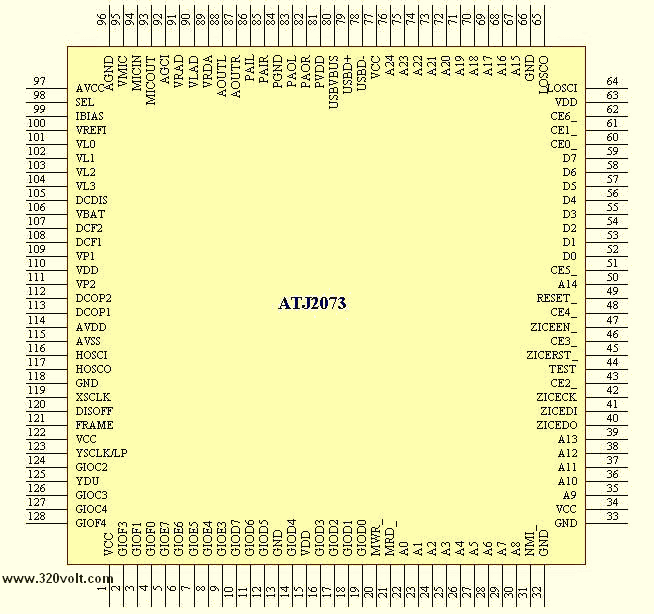
ATJ2073 LQFP128 Datasheet pinout
ATJ2073 LQFP128 Datasheet
The ATJ2073 is a single-chip highly-integrated digital music system solution for devices such as dedicated audio players, PDAs, and cell phones. It includes an audio decoder with a high performance DSP with embedded RAM, ADPCM/AG record capabilities and USB interface for downloading music and uploading voice recordings. ATJ2073 also provides an interface to S/PDIF audio data input, flash memory, LED/LCD, button and switch inputs, headphone, and microphone, and FM radio control.
The ATJ2073’s programmablearchitecture supports the MP3 and other digital audio standards. For devices like USB Flash Disk, the ATJ2073 can act as a USB mass storage slave device to personal computer system. The ATJ2073 has low power consumption to allow long battery life and an efficient flexible on-chip DC-DC converter that allows many different battery configurations, including 1xAA, 1xAAA, 2xAA,2xAAA.
ATJ2115F pin out bağlantı şeması
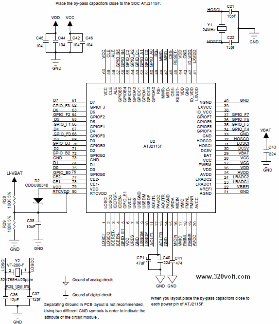
ATJ2115F-schematic-pinout ATJ2115F datasheet, ATJ2115F schematic, ATJ2115F
Rock chip RK2608A Pinout bağlantı şeması
Rockchip RK2608A schematic Rock chip RK2608A, Rockchip, RK2608A datasheet, RK2608A schematic
ACU7512 Bağlantı şeması
ACU7512 Bir çok mp4, mp3 oynatıcıda kullanılıyor usb, sd kart vb gibi bir çok
multi medya özelliği var tam data sheet dosyası verilmiyor ama bağlantı
şeması az çok işe yarar
ATJ2085 Datasheet pinout
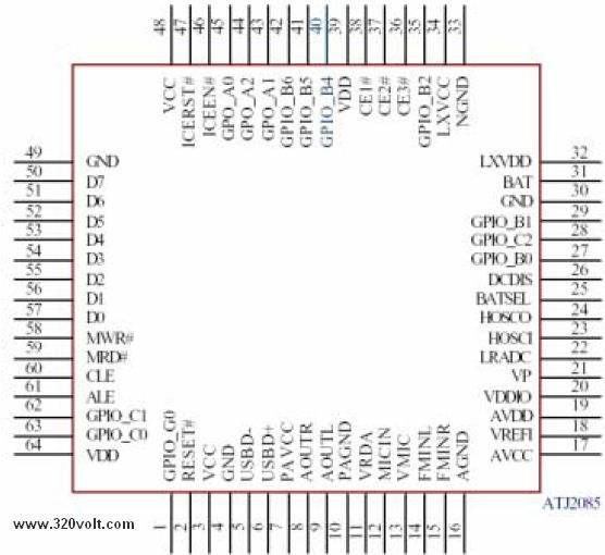
ATJ2085 Datasheet pinout
ATJ2085 is a single-chip for flash-based digital music player. It includes an audio decoder with a high performance DSP, ADPCM record capabilities and USB interface for downloading music and uploading voice recordings. ATJ2085 also provides an interface to flash memory, LED, button and switch inputs, headphone, and microphone, and FM radio input and control. ATJ2085’s programmable architecture supports the MP3, WMA
and other digital audio standards.
For devices like USB-Disk, ATJ2085 can act as a USB mass storage slave device to personal computer system. Its low power consumption allows a long battery life, and an efficient flexible on-chip DC-DC converter allows many different battery configurations, including 1xAA, 1xAAA, 2xAA, 2xAAA and Li-Ion. Built-in Sigma-Delta DAC & a headphone driver to directly drive low impedance headphones. The ADC includes inputs for both Microphone and Analog Audio in to support voice recording and FM radio integration features.
ATJ2111L pin out bağlantı şeması
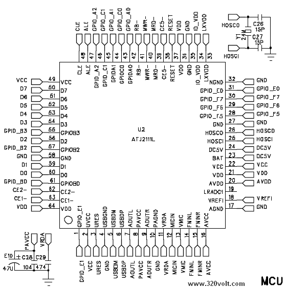
ATJ2111L-schematic-pinout ATJ2111L datasheet, ATJ2111L, ATJ2111L schematic

Sharp LM64P89 LM64P839
| Display type: | Sharp LM64P89 & LM64P839 | ||
|---|---|---|---|
| Inverter no.: | 40900097 | ||
| Cable no.: | 72560100 | ||
| System: | 686LCD with FPUM-2 and AC-2 | ||
| Display driver: | SHA LM64K836 | ||
| Status: | Verified | ||
| Display | Connector | JPLCD | 50-pole connector | Remarks |
| Term. # | Function | Pin | Connector | |
| 1 | S | 11 | FLM | Scan start-up signal |
| 2 | CP1 | 10 | LP | Input data latch signal |
| 3 | CP2 | 13 | SHFCLK | Data input clock signal |
| 4 | DISP | 8 | CPO1 | Display control signal |
| 5 | VDD | 2 | VCC | Power supply for logic and LCD (+5V) |
| 6 | VSS | 38 | GND | Ground potential |
| 7 | VEE | 40 | VEE | power supply for LCD (-) |
| 8 | DU0 | 19 | P3 | Display data signal (Upper half) |
| 9 | DU1 | 18 | P2 | |
| 10 | DU2 | 16 | P1 | |
| 11 | DU3 | 15 | P0 | |
| 12 | DL0 | 25 | P7 | Display data signal (Lower half) |
| 13 | DL1 | 24 | P6 | |
| 14 | DL2 | 22 | P5 | |
| 15 | DL3 | 21 | P4 |
AK1025 bağlantı şeması

AK1025 datasheet, AK1025
ATJ2097 pinout cpu bağlantı şeması
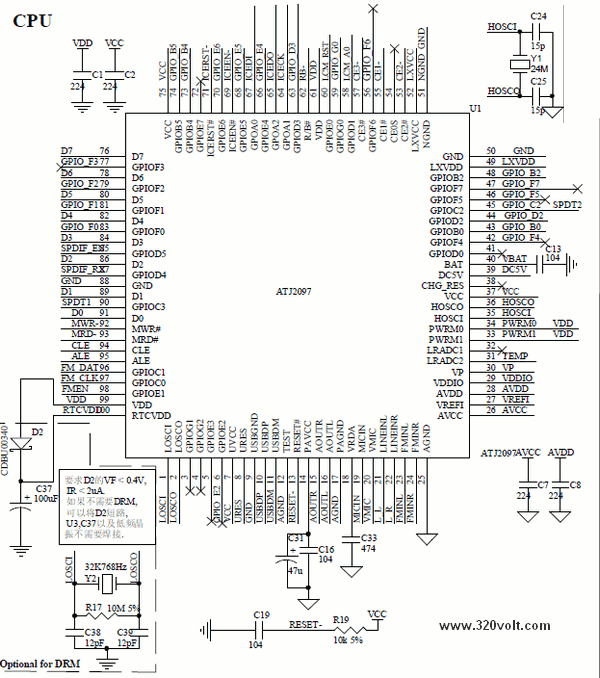
ATJ2097-schematic-pinout ATJ2097 datasheet, ATJ2097 schematic, ATJ2097
ATJ2087 Pinout bağlantı şeması
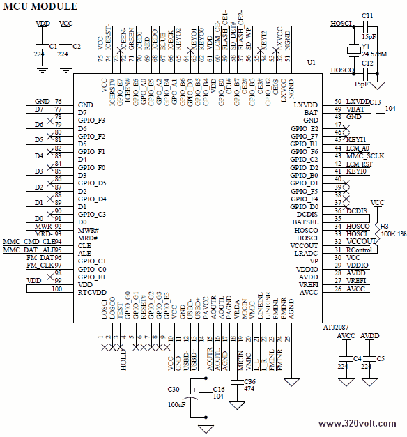
ATJ2087 diagram ATJ2087 pinout ATJ2087 datasheet, ATJ2087 pinout, ATJ2087
ACU7502 Datasheet (pin connection)
acu7502 datasheet, acu7502
ATJ2001 LQFP176 bağlantı şeması
ATJ2001 LQFP176 pin
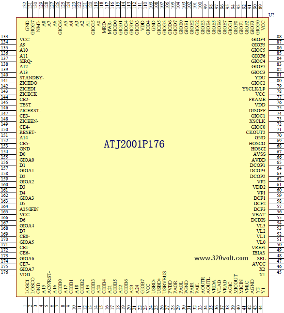
ATJ2001, LQFP176, ATJ2001 datasheet, LQFP176 datasheet
ATJ2091 pinout bağlantı şeması
ATJ2091 schematic ATJ2091 pinout ATJ2091 schematic, ATJ2091 pinout, ATJ2091 datasheet
ATJ2007 Mcu modül şeması
ATJ2007 pin out ATJ2007 datasheet, ATJ2007 schematic, ATJ2007
ACU7502 Datasheet (pin connection)
ATJ2055 Datasheet
ATJ2055 Datasheet
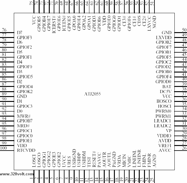
ATJ2063N Datasheet
ATJ2063N Data sheet
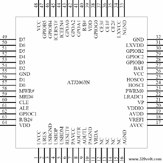
ACU7515 cpu bağlantı şeması

ATJ2051 Datasheet
ATJ2051 Data sheet
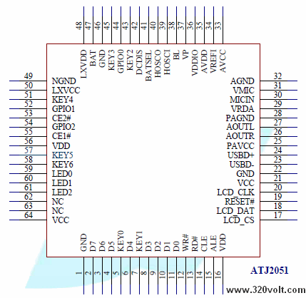
ATJ2051X is a single-chip for flash-based digital music player. It includes an audio decoder with a high performance DSP, ADPCM record capabilities and USB interface for downloading music and uploading voice recordings. ATJ2051X also provides an interface to flash memory, button and switch inputs, headphone, and microphone. ATJ2051X’s programmable architecture supports the MP3, WMA and other digital audio standards.
For devices like USB-Disk, ATJ2051X can act as a USB mass storage slave device to personal computer system. Its low power consumption allows a long battery life, and an efficient flexible on-chip DC-DC converter allows many different battery configurations, including 1xAA, 1xAAA, 2xAA, 2xAAA and Li-Ion. Built-in Sigma-Delta DAC & a headphone
driver to directly drive low impedance headphones. The ADC includes inputs for both Microphone and Analog Audio in to support voice recording features. Thus, the ATJ2051X provides a true ‘ALL-IN-ONE’ solution that is ideally suited for highly optimized digital audio
players with mass storage function.
STMP36XX BGA Pinout uygulama şeması
stmp36xx-bga-schematic-pin-out stmp36xx datasheet, stmp36xx schematic, stmp36xx bga
ATJ2093 Pinout bağlantı şeması
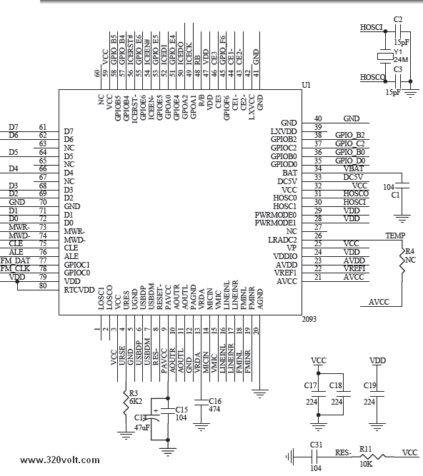
atj2093-cpu-schematic-pinout atj2093 datsheet, atj2093 schematic, atj2093 pinout
ACU7517 bağlantı şeması
ATJ2092H Data Sheet pinout
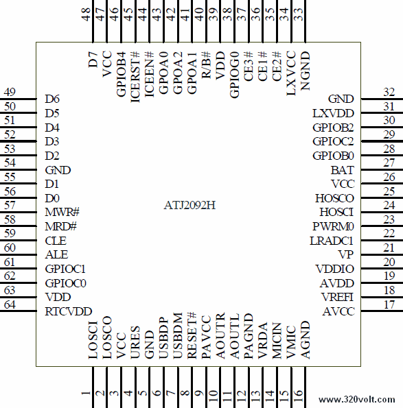
ATJ2092H Datasheet pinout
ATJ2092H is a new generation single-chip highly-integrated digital multimedia SOC for devices such as dedicated audio players, photo viewers, PDAs. It includes audio codec, image and video decoding engine, a high performance 2 core (DSP and MCU) structure with embedded RAM and ROM, digital record capabilities and USB interface for downloading and uploading. ATJ2092H also provides an interface to flash memory,
LED/LCD/OLED, button and switch inputs, headphones, microphone.
ATJ2092H contains a high performance DSP, which can easily be programmed to support many kinds of digital audio standards such as MP3, WMA, etc. As storage devices ATJ2092H can act as a USB mass storage slave device to personal computer system and meanwhile ATJ2092H can be applied as MTP. ATJ2092H has low power consumption
ACU75032 bağlantı şeması
Rockchip RK2606A Pinout bağlantı şeması
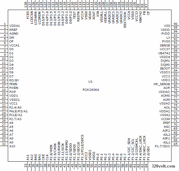
Rock chip-RK2606A-pin-out Rockchip RK2606A, RK2606A datasheet, RK2606A schematic
ATJ2093 Pinout bağlantı şeması

atj2093-cpu-schematic-pinout atj2093 datsheet, atj2093 schematic, atj2093 pinout
Actions ACU7503 Datasheet (pin connections)
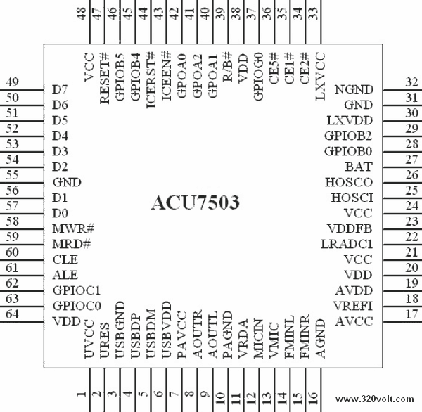
Instruction set of MCU compatible with Z80, Internal SRAM access time<7ns, MROM access time<16ns, Accurate Clock Management Unit, supplies 24MHz OSC, Energy saving Power Management Unit, supports 1xAA, 1xAAA, 2-channel DMA, 1-channel Counter/Timer Controller and Interrupt Controller, Support USB 2.0 high speed, acting as mass storage deviceSupport up to 4(pcs)*64M-4G bytes Nand type SLC/MLC Flash, Built-in Key Scan Circuit and GPIOs, Built-in Stereo Sigma-Delta DAC and ADC Digital voice recording at ultra low 4.4 or 8Kbps with Actions Speech Algorithm, upport FM Radio input and 32 levels volume control, Support extended low frequency crystal to generalize RTC 0.18um 1P5M CMOS process and packaged at LQFP-80(10*10mm)
| Pin No. | Pin Name | I/O Type | Driver Capacity | Reset Default | Short Description |
|---|---|---|---|---|---|
| 1 | UVCC | PWR | / | / | Power supply for USB |
| 2 | URES | AO | / | / | USB precision Resistor |
| 3 | USBGND | PWR | / | / | USB ground |
| 4 | USBDP | A | / | H | USB data plus |
| 5 | USBDM | A | / | H | USB data minus |
| 6 | USBVDD | PWR | / | / | USB power |
| 7 | PAVCC | PWR | / | / | Power supply for Power Amplifier |
| 8 | AOUTR | AO | / | / | Int. PA right channel analog output |
| 9 | AOUTL | AO | / | / | Int. PA left channel analog output |
| 10 | PAGND | PWR | / | / | Power Amplifier ground |
| 11 | VRDA | AO | / | / | Bypass capacitor connect pin for int. DAC Reference voltage |
| 12 | MICIN | AI | / | / | Microphone pre-amplifier input |
| 13 | VMIC | PWR | / | / | Power supply for Microphone |
| 14 | FMINL | AI | / | / | Left channel of FM line input |
| 15 | FMINR | AI | / | / | Right channel of FM line input |
| 16 | AGND | PWR | / | / | Analog ground |
| 17 | AVCC | PWR | / | / | Power supply of analog |
| 18 | VREFI | AI | / | / | Voltage reference input |
| 19 | AVDD | PWR | / | / | Analog core power pin |
| 20 | VDD | PWR | / | Z | Core power |
| 21 | VCC | PWR | / | / | IO power |
| 22 | LRADC1 | AI | / | / | Low resolution A/D input 1 |
| 23 | VDDFB | AI | / | / | VDD feedback |
| 24 | VCC | PWR | / | / | IO power |
| 25 | HOSCI | AI | / | / | High frequency crystal OSC input |
| 26 | HOSCO | AO | / | / | High frequency crystal OSC output |
| 27 | BAT | I | / | / | Battery voltage input. |
| 28 | GPIO_B0 | BI | 2mA | Z | Bit0 of General Purpose I/O port B |
| KEYI0 | I | H | Bit0 of key scan circuit input | ||
| CE3- | O | H | Chip enable 3 |
| 29 | GPIO_B2 | BI | 2mA | Z | Bit2 of General Purpose I/O port B |
|---|---|---|---|---|---|
| KEYI2 | I | H | Bit2 of key scan circuit input | ||
| CE4- | O | H | Chip enable 4. | ||
| 30 | LXVDD | PWR | / | / | VDD DC-DC pin |
| 31 | GND | PWR | / | / | Ground |
| 32 | NGND | PWR | / | / | NMOS ground |
| 33 | LXVCC | PWR | / | / | VCC DC-DC pin |
| 34 | CE2- | O | NF_PAD | H | Ext. memory chip enable 2 |
| 35 | CE1- | O | NF_PAD | H | Ext. memory chip enable 1 |
| 36 | CE5- | O | 4mA | H | Ext. memory chip enable 5 |
| GPO_A3 | BI | / | Bit3 of General Purpose Output port A | ||
| 37 | GPIO_G0 | BI | 2mA | Z | Bit0 of General Purpose I/O port G |
| MMC_CMD | O | / | Command/Respond of SD/MMC | ||
| 38 | VDD | PWR | / | / | Digital core power |
| 39 | RB- | I | 4mA | H | Nand Flash Ready/Busy status input |
| 40 | GPO_A1 | O | 4mA | L | Bit1 of General Purpose Output port A |
| ICECK | I | / | Clock input of DSU | ||
| 41 | GPO_A2 | O | 4mA | L | Bit2 of General Purpose Output port A |
| ICEDO | O | / | Data output of DSU | ||
| 42 | GPO_A0 | O | 4mA | 0 | Bit0 of General Purpose Output port A |
| ICEDI | I | / | Data input of DSU | ||
| 43 | ICEEN- | I | 4mA | / | DSU enable (active low) |
| 44 | ICERST- | I | 4mA | / | DSU reset (active low) |
| 45 | GPIO_B4 | BI | 2mA | Z | Bit4 of General Purpose I/O port B |
| KEYO0 | O | / | Bit0 of key scan circuit output | ||
| 46 | GPIO_B5 | BI | 2mA | Z | Bit5 of General Purpose I/O port B |
| KEYO1 | O | / | Bit1 of key scan circuit output | ||
| 47 | RESET- | I | USCU | H | System reset input (active low) |
| 48 | VCC | PWR | / | / | Digital power pad |
| 49 | D7 | BI | NF_PAD | L | Bit7 of ext. memory data bus |
| 50 | D6 | BI | NF_PAD | L | Bit6 of ext. memory data bus |
| 51 | D5 | BI | NF_PAD | L | Bit5 of ext. memory data bus |
| 52 | D4 | BI | NF_PAD | L | Bit4 of ext. memory data bus |
| 53 | D3 | BI | NF_PAD | L | Bit3 of ext. memory data bus |
| 54 | D2 | BI | NF_PAD | L | Bit2 of ext. memory data bus |
| 55 | GND | PWR | / | / | Ground |
|---|---|---|---|---|---|
| 56 | D1 | BI | NF_PAD | L | Bit1 of ext. memory data bus |
| 57 | D0 | BI | NF_PAD | L | Bit0 of ext. memory data bus |
| 58 | MWR | O | NF_PAD | H | Ext. memory write strobe |
| 59 | MRD- | O | NF_PAD | H | Ext. memory read strobe |
| 60 | CLE | O | NF_PAD | L | Command Latch Enable fo NandFlash |
| 61 | ALE | O | NF_PAD | L | Address latch enable for NAND flash |
| 62 | GPIO_C1 | BI | 2mA | OD | Bit1 of General Purpose I/O port C |
| I2C_SDA | O | / | I2C Serial data (Open drain) | ||
| SIRQ- | I | / | Ext. interrupt request input | ||
| 63 | GPIO_C0 | BI | 2mA | OD | Bit0 of General Purpose I/O port C |
| I2C_SCL | O | / | I2C serial clock (Open drain) | ||
| 64 | VDD | PWR | / | / | Digital core power |

