There are two versions of the Ni-cd charging circuit, one with bjt (mje2955) transistor and the other with mosfet (2sj295). There is not much difference between the output transistor changed. D1 led shows the power supply input. D2 led shows the battery is full. D3 led shows that the battery is connected to the circuit.
The charging current can be increased by changing the value of the R8 resistor in the circuit. It is an ideal quality charging circuit especially for people who are dealing with nicad battery powered drills, chargers, model mock-ups. The author has already shared the circuit he uses in his models.
| Charge current | R8 | R8 power |
|---|---|---|
| 250ma | 3.3Ω | 05w |
| 500ma | 1.5Ω | 1w |
| 1a | 0.68Ω | 2w |
| 1.5a | 0.47Ω | 2w |
| 2a | 0.33Ω | 3w |
The Nicad charger will charge 1 to 7 cells up to 2 Amps when powered with 12V. If you have access to a higher voltage power source, more cells can be charged. To calculate how much voltage is required, let’s assume 1.6 V per cell plus 0.8 V loop loss. Therefore, you will need at least (1.6*10)+0.8=16.8V to charge 10 cells.
The circuit consists of two parts, a constant current generator using a PNP power transistor (Q2) and a peak detection shutdown circuit using a high gain LM358 opamp. To initiate the charge cycle, switch SW1 is momentarily closed, causing C1 to discharge. Since IC1’s inverting input is now higher than its non-inverting input, its output goes low and turns on Q1. This lights up the red “charge” LED (D2) and supplies about 80mA through R6 and R7 to turn on Q2 which is starting to charge the battery. The charging current flows through R8 on its way to the battery. When the voltage across R8 exceeds about 0.6V, Q3 starts to turn on and steals current from the base of Q2. This regulates the output current by an amount determined by the value of R8.

We take advantage of the ‘peak’ effect of a Nicad battery to detect the discharge. During charging, the voltage in the battery rises continuously until no more charge can be stored; At this point, the excess energy must be dissipated as heat. The resulting increase in battery temperature causes the voltage to drop slightly (as little as 7 mV per cell). In this circuit, peak detection is achieved by comparing the battery voltage with a time-delayed version stored in capacitor C1. When the battery voltage goes up, the voltage across C1 lags behind the voltage at C3, thus keeping the IC1 output low. If the voltage at C1 is higher than at C3, the battery voltage should now be dropping. Since IC1’s non-inverting input is now higher than its inverting input, its output rises, turning Q1 off and stopping the charge cycle.
The Q4 monitors the charge current to ensure that the output current is kept off at the end of the charge. If the current drops below half the preset amount, Q4 will turn on and force the non-inverting IC1 input high, thus permanently stopping charging. This happens on peak detection or if the battery voltage gets too close to the supply voltage (eg if the battery is disconnected). Along with R11 and R12, the orange “power” indicator LED (D3) provides a voltage reference of 0.9 V based on Q4. By subtracting 0.6V between base and emitter, Q4 turns on when the voltage across R8 drops below 0.3V.
Unfortunately, the inputs of an LM358 opamp only work properly down to 1.5 V less than the supply voltage. It is necessary to keep the opamp inputs below this level to make full use of the available power supply voltage. When the battery under charge reaches 10V, R9 drops by about 1.5V (due to current flowing through R5 and D5). It drops progressively less at lower voltages, so it doesn’t reduce sensitivity unnecessarily.
Another problem is that the output of an LM358 doesn’t go all the way to the supply rail, but it can only manage below about 1.2 V. Therefore, Q1 and Q2 may not turn off completely, causing the “battery” LED to stay lit when it shouldn’t. Therefore, R14 has been added to ensure that Q2 is fully closed.
If you try to charge a battery that is already full, it can peak very quickly. Since the time constant of R3 and C2 is quite long (more than 20 seconds), D4 was added to allow C2 to reach at least 90% charge immediately, so that the peak sensing circuit “prepared” for discharge to not miss the signal.
Added a few more parts to increase reliability. C5 and R10 ensure high frequency stability of the current regulator, C4 and C6 smooth out the power supply noise, and C1 and C3 eliminate noise in the sensitive peak detection circuit. R1, R2 and R10 limit overcurrents through Q4, SW1 and Q3, respectively.
I designed this circuit to use off-the-shelf parts, no expensive or exotic ICs required! Many different opamps can be used for the IC1, just make sure the common mode input voltage range, output swing and bias current are good enough. The bias current should be less than 100nA. Input offset voltage should be less than 3mV. This can be achieved by choosing a high-spec part like the LM358A or AD708 (better), a null-tuned opamp (a trim-pot needs to be added), or a single part for low offset voltage. Transistors can be pretty much any type as long as they’re PNP, have reasonable current gain, and can handle power.
D1, D2 and D3 LEDs can be any color you want. I used yellow for “power”, red for “charge” and green for “battery”. Check the voltage drop across R11 and adjust its value to 0.9V if necessary. Some LEDs drop different voltages, eg. Blue LEDs typically use about 4V, compared to 1.8V for a red or yellow LED and 2.2V for green.
Q2 can be quite hot and may need a cooler depending on the number of batteries.
Nickel–cadmium battery charger

Charging 6 cells or less at high current as it needs to absorb excess voltage. It should be mounted on a good heatsink. Resistors R7 and R8 will also get quite hot. Do not use lower grades than specified.
C2 should have low leakage. This is very important as excessive leakage current through this capacitor will reduce peak detection sensitivity. Electrolytics often suffer from this problem, especially if they have been stored for a long time. Leakage can often be reduced by ‘building up’ the capacitor, you do this by applying operating voltage for a few hours. Tantalum capacitors have lower leakage, but are difficult to get large sizes (you may need to connect several in parallel to create the required value).
Setting Charge Current
By adjusting the value of R8, the charging current can be adjusted to suit your battery. You can connect a switch to select a suitable resistor for each desired current. Most Nicads can be safely charged in 30 minutes, which corresponds to twice their capacity, or 2C (for example, a 300mAh cell can be charged at 600mA). With a 12 V supply, a 7-cell pack may need to be charged at a lower rate to keep the peak voltage below 11.2 V (1.6 V per cell), otherwise premature shutdown may occur. It is not recommended to charge at current less than 1C, as the peak effect is very weak and can be overlooked.
Current R8 (Ohm) rating
250mA 3.3 0.5W
500mA 1.5 1W
1A 0.68 2W
1.5A 0.47 2W
2A 0.33 3W
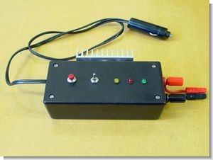
These pictures show my charger plugged into a small project box and the heatsink mounted outside for better cooling. Three-position switch selects 500mA, 1A or 2A charging currents. The output terminals can take bare wires or banana plugs (a short wire with Sermos connector is attached in the photos).
For convenience, I’ve built the circuit in Veroboard, which is good for prototyping but prone to assembly errors. Therefore, I have now designed a single-sided PCB. Note that I haven’t tested this board layout yet. If you think there are any errors in it, please let me know! The board dimensions are 2.5 x 2.5 inches and should be actual size when printed at 300 dpi (to download the image, click the thumbnail to see the full image, then right click and select ‘Save image as’).
Connect an appropriate DC power supply to the 12V Supply inputs that will illuminate the “Power” LED. Now connect your Nicad pack to the output (taking care of the correct polarity!). Provided the pack voltage is at least 2.4 V, the “battery” LED should illuminate (if it is not, there is either a bad connection or polarity reversed). Press the “Start” button for one second and the “charge” LED should light up. Wait for Nicad to peak, at which time the “Charge” LED should go out.
DO NOT leave a charging battery unattended! Check the package temperature regularly. If charging does not stop automatically after a reasonable time or the pack becomes hot, disconnect it immediately. If charging stops too soon, one cell in your pack may have peaked earlier than the others, so you can hit the “Start” button again. However, do not reboot if the package is hot.
Disconnect the pack immediately after charging to avoid slow discharge to the “Battery” LED (a 600mAh 7.2V pack loses about 1% charge per hour).
Wouldn’t it be nice to have an audible indicator instead of periodically checking the LEDs to see when the charge is running out? This circuit makes…
CHRG is taken from pin 1 of the LM358 opamp on the charger. At boot, /CHRG is high, so IC1A output is low and IC1B output stays high. Pressing the ‘Start’ button will decrease /CHRG. IC1A reverses this and causes C3 to start charging through R2. After about 2 seconds the voltage across C3 is high enough to activate the oscillator created by IC1B, C1 and R1. This produces a square wave with a frequency of about 2kHz, which is fed into the IC1D. However, /CHRG is also connected to the IC1D, preventing the 2kHz tone from reaching the piezo speaker. At the end of the charge, /CHRG will turn high, but the oscillator will continue to run until C3 is discharged (for another 2 seconds). The IC1D is now active, so the speaker is enabled. The IC1C doubles the voltage to the speaker for more noise!
The circuit is simple enough to be assembled on a small board. The +12V power supply is connected to pin 14 of IC1 and Ground goes to pin 7.
Using P channel MOSFET for Higher Current

The original circuit’s charging current is limited to 2A, not because the output transistor can handle more, but because it needs a lot of base current. FETs are controlled by voltage rather than current, so they have much lower driver requirements.
Replacing the bipolar output transistor with a P-Channel MOSFET provides as high a charge current as the FET can withstand (with an appropriate R8 value, eg 5 Ohms for 0.1 4A). Both R8 and FET can get very hot at high currents so make sure they are adequately rated and have heatsinks! Charging less than 4 cells at 4A is impractical because the FET gets very hot.
Note that the values for R7 and R14 have changed and R6 is now connected to the positive supply rail.
There is a pcb drawing of the circuit prepared with eagle cad;
source homepages.paradise.net.nz/bhabbott/charger.html High-current Nicad Battery Charger Circuit schematic pcb files alternative link :
Password: 320volt.com
Published: 2009/12/06 Tags: battery charger circuit, power electronic projects
4-Channel Car Amplifier Circuit TDA1558Q
TDA1558Q 4×11 watt amplifier circuit can be installed with very little material prepared by the eagle of the circuit diagram, pcb drawings there. 2 × 22 watt with a few changes can be used as an integrated amp or 5.1 audio prompt auto low power outputs (fr, fl, rr, rl) is ideal.
TDA1558Q IC implemented, would like to introduce 4-channel amplifier. But due to the design of methods are that bridged, or even start using a stereo amplifier. In this article we discuss the implementation as well.
Why is this the ICs I chose? There are several reasons. First, as is primarily intended for in-car use, such as the supply of a PC power supply can be easily solved. On the other hand, if you do that we build two, then one of them is all it bridged a 5.1 amp. (In this case of course it does not hurt to do a low-pass filter in front of the deep-channel input.)