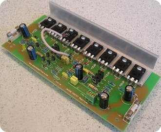
A beautiful design power and operating voltage pretty high 🙂 detailed explanation (in English) diagrams and PCB files are photos of a top version, but not much change
According to the calculations used transformer power 625W output voltage 2x50v total 100v ac Be careful, high voltage Rectifier post dc voltage 70V DC + – 2x70v = 140V dc (50 x 1:41) rectification is used to bridge diode 35 amp metal type filter capacitors + – channel two per 10,000 uF 100volt
400 Watts RMS

Anfi is used at the output 200w 8Ω 4Ω speaker with a 400w is powering noise ratio 0.005% THD 4 Mosfets IRFP240 used and 4 IRFP9240
200 Watts RMS into 8 Ohms
400 Watts RMS into 4 Ohms
Total Harmonic Distortion is typically 0.005%,
Signal to Noise Ratio of -122dB unweighted (20Hz to 20Khz)
A-weighted -126dB Damping Factor Greater than 200 at 8 Ohms
400w Mosfet Amplifier Circuit Diagram

Construction notes for the symmetrical 400 watt amplifier. The symmetric amplifier is an update of my designs published in the Australian electronics magazine Silicon Chip in June 1994.
The main changes made to this design were the addition of a clipping detector circuit and bias circuit modifications for the use of International Rectifier HEXFET MOSFETs.
Subsequent changes to the error amp and VAS stages that improve the overall sound of the amplifier. Tools you will need to complete the build of this module
The first stage is what I call an asymmetric input error amplifier. It is only capable of accepting an unstable I/P source. I will now describe how each device at this stage works together.
Q2, Q3, R35-R36 form the main differential error amplifier, and then their collectors are connected to a cascade load. Q4, Q5, R4 and ZD2 form the cascode stage, providing a constant 14.4 volts at the collectors Q4, Q5.
Q1, R8, R7, ZD1 and C1 form a constant current source that supplies 1.5 milliamps to the first differential stage. These modules form the first stage of the amplifier and basically adjust how the entire amplifier is biased from front to back.
This next stage provides most of the voltage amplification needed by the next stage to get the o/p stage to full power. Q6, Q7, Q8, Q9, R15, R14, R12, R13, C3, C7, C8 form the second differential voltage amplification stage. Q7 and Q9 form what is known as the current mirror load for the second differential stage, basically forcing that stage to share the current supplied from R15, which is about 8 milliamps.
The remaining components, namely the caps, provide local frequency compensation for this stage. As the name suggests, Q10, R34, 37, 38, C12 form the bias stage. Its main purpose is to provide a stable and compensated supply voltage to the MOSFET Gates.
Once again, as the name suggests, this stage converts the voltage developed in the VAS and provides all the amps needed to drive 8 or 4 Ohm loads. 2-Ohm loads are not possible unless more o/p devices are added.
Mosfet Amplifier 400w project belongs to the pcb, schema files:
Password: 320volt.com
Published: 2008/02/12 Tags: audio amplifier circuits, transistor amplifier
PIC12F675 PC Programmable Security System
This project uses the 12F675, it was chosen because of its low cost, A/D convertor and flash memory. This security system was designed to be used in a simple installation with just a hidden switch and not a keyboard. There are several features such as a battery monitor built into the code that also make it good for remote locations just run off a battery. Also all the delays and and other parameters are put into flash memory just by using a visual basic program and the serial port of a PC.
Ein schönes Design Leistung und Betriebsspannung ziemlich hoch 🙂 Detaillierte Erklärung (in Englisch) Diagramme und PCB-Dateien sind Fotos einer Top-Version, aber nicht viel zu ändern
Nach den Berechnungen verwendet Transformatorleistung 625W Ausgangsspannung 2x50V insgesamt 100V AC Vorsicht, Hochspannung Gleichrichter nach Gleichspannung 70V DC + – 2x70V = 140V DC (50 x 1:41) Gleichrichtung wird verwendet, um Dioden 35 Ampere Metallfilterkondensatoren zu überbrücken + – Kanal zwei pro 10.000 uF 100 Volt